- 您现在的位置:买卖IC网 > PDF目录11202 > ADUC816BCPZ (Analog Devices Inc)IC MCU FLASH 16BIT ADC 56LFCSP PDF资料下载
参数资料
| 型号: | ADUC816BCPZ |
| 厂商: | Analog Devices Inc |
| 文件页数: | 15/68页 |
| 文件大小: | 0K |
| 描述: | IC MCU FLASH 16BIT ADC 56LFCSP |
| 标准包装: | 1 |
| 系列: | MicroConverter® ADuC8xx |
| 核心处理器: | 8052 |
| 芯体尺寸: | 8-位 |
| 速度: | 12.58MHz |
| 连通性: | I²C,SPI,UART/USART |
| 外围设备: | PSM,温度传感器,WDT |
| 输入/输出数: | 34 |
| 程序存储器容量: | 8KB(8K x 8) |
| 程序存储器类型: | 闪存 |
| EEPROM 大小: | 640 x 8 |
| RAM 容量: | 256 x 8 |
| 电压 - 电源 (Vcc/Vdd): | 2.7 V ~ 5.5 V |
| 数据转换器: | A/D 7x16b; D/A 1x12b |
| 振荡器型: | 内部 |
| 工作温度: | -40°C ~ 85°C |
| 封装/外壳: | 56-VFQFN 裸露焊盘,CSP |
| 包装: | 托盘 |
第1页第2页第3页第4页第5页第6页第7页第8页第9页第10页第11页第12页第13页第14页当前第15页第16页第17页第18页第19页第20页第21页第22页第23页第24页第25页第26页第27页第28页第29页第30页第31页第32页第33页第34页第35页第36页第37页第38页第39页第40页第41页第42页第43页第44页第45页第46页第47页第48页第49页第50页第51页第52页第53页第54页第55页第56页第57页第58页第59页第60页第61页第62页第63页第64页第65页第66页第67页第68页
REV. 0
ADuC816
–22–
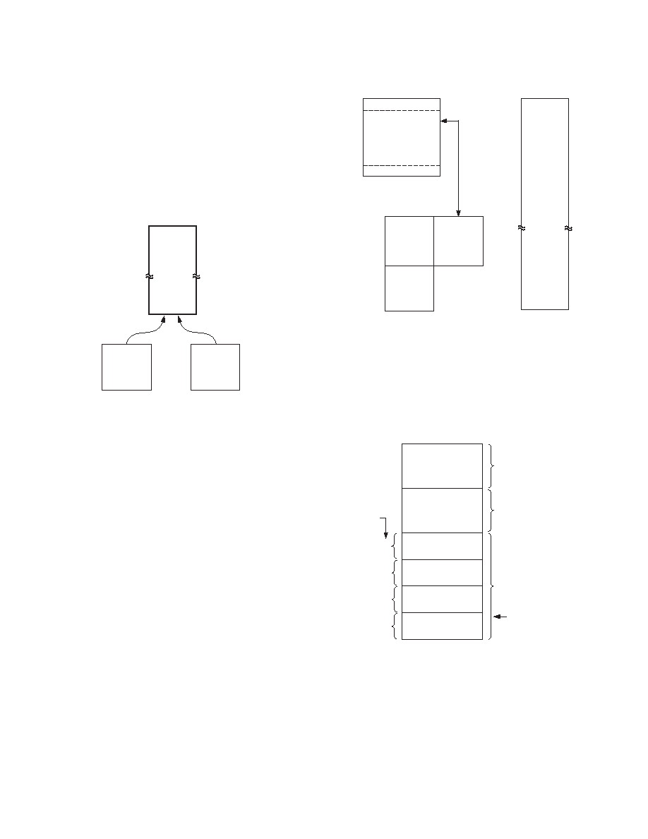
MEMORY ORGANIZATION
As with all 8051-compatible devices, the ADuC816 has sepa-
rate address spaces for Program and Data memory as shown in
Figure 13 and Figure 14.
If the user applies power or resets the device while the
EA pin is
pulled low, the part will execute code from the external pro-
gram space, otherwise the part defaults to code execution
from its internal 8 Kbyte Flash/EE program memory. This
internal code space can be downloaded via the UART serial
port while the device is in-circuit.
EXTERNAL
PROGRAM
MEMORY
SPACE
FFFFH
2000H
1FFFH
0000H
EA = 1
INTERNAL
8 KBYTE
FLASH/EE
PROGRAM
MEMORY
PROGRAM MEMORY SPACE
READ ONLY
EA = 0
EXTERNAL
PROGRAM
MEMORY
SPACE
Figure 13. Program Memory Map
The data memory address space consists of internal and exter-
nal memory space. The internal memory space is divided into
four physically separate and distinct blocks, namely the lower
128 bytes of RAM, the upper 128 bytes of RAM, the 128 bytes
of special function register (SFR) area, and a 640-byte Flash/EE
Data memory. While the upper 128 bytes of RAM, and the
SFR area share the same address locations, they are accessed
through different address modes.
The lower 128 bytes of data memory can be accessed through
direct or indirect addressing, the upper 128 bytes of RAM can
be accessed through indirect addressing, and the SFR area is
accessed through direct addressing.
Also, as shown in Figure 13, the additional 640 Bytes of
Flash/EE Data Memory are available to the user and can be
accessed indirectly via a group of control registers mapped into
the Special Function Register (SFR) area. Access to the Flash/
EE Data Memory is discussed in detail later as part of the Flash/
EE Memory section in this data sheet.
The external data memory area can be expanded up to 16 MBytes.
This is an enhancement of the 64 KByte external data memory
space available on standard 8051-compatible cores.
The external data memory is discussed in more detail in the
ADuC816 Hardware Design Considerations section.
SPECIAL
FUNCTION
REGISTERS
ACCESSIBLE
BY DIRECT
ADDRESSING
ONLY
640 BYTES
FLASH/EE DATA
MEMORY
ACCESSED
INDIRECTLY
VIA SFR
CONTROL REGISTERS
INTERNAL
DATA MEMORY
SPACE
FFH
80H
7FH
00H
UPPER
128
FFH
80H
EXTERNAL
DATA
MEMORY
SPACE
(24-BIT
ADDRESS
SPACE)
000000H
DATA MEMORY SPACE
READ/WRITE
(PAGE 159)
(PAGE 0)
00H
9FH
FFFFFFH
LOWER
128
ACCESSIBLE
BY
INDIRECT
ADDRESSING
ONLY
ACCESSIBLE
BY
DIRECT
AND INDIRECT
ADDRESSING
Figure 14. Data Memory Map
The lower 128 bytes of internal data memory are mapped as shown
in Figure 15. The lowest 32 bytes are grouped into four banks
of eight registers addressed as R0 through R7. The next 16 bytes
(128 bits), locations 20Hex through 2FHex above the register
banks, form a block of directly addressable bit locations at bit
addresses 00H through 7FH. The stack can be located anywhere
in the internal memory address space, and the stack depth can be
expanded up to 256 bytes.
BIT-ADDRESSABLE
(BIT ADDRESSES)
FOUR BANKS OF EIGHT
REGISTERS
R0 R7
BANKS
SELECTED
VIA
BITS IN PSW
11
10
01
00
07H
0FH
17H
1FH
2FH
7FH
00H
08H
10H
18H
20H
RESET VALUE OF
STACK POINTER
30H
GENERAL-PURPOSE
AREA
Figure 15. Lower 128 Bytes of Internal Data Memory
REV. A
相关PDF资料 |
PDF描述 |
|---|---|
| VE-B3H-IX-F1 | CONVERTER MOD DC/DC 52V 75W |
| VE-B44-IW | CONVERTER MOD DC/DC 48V 100W |
| VE-B3H-IW-F4 | CONVERTER MOD DC/DC 52V 100W |
| VE-B3H-IW-F2 | CONVERTER MOD DC/DC 52V 100W |
| VE-B3H-IW-F1 | CONVERTER MOD DC/DC 52V 100W |
相关代理商/技术参数 |
参数描述 |
|---|---|
| ADUC816BCPZ-REEL | 功能描述:8052 MicroConverter? ADuC8xx Microcontroller IC 8-Bit 12.58MHz 8KB (8K x 8) FLASH 56-LFCSP (8x8) 制造商:analog devices inc. 系列:MicroConverter? ADuC8xx 包装:带卷(TR) 零件状态:上次购买时间 核心处理器:8052 核心尺寸:8-位 速度:12.58MHz 连接性:I2C,SPI,UART/USART 外设:PSM,温度传感器,WDT I/O 数:34 程序存储容量:8KB(8K x 8) 程序存储器类型:闪存 EEPROM 容量:640 x 8 RAM 容量:256 x 8 电压 - 电源(Vcc/Vdd):2.7 V ~ 5.5 V 数据转换器:A/D 7x16b;D/A 1x12b 振荡器类型:内部 工作温度:-40°C ~ 85°C(TA) 封装/外壳:56-WFQFN 裸焊盘,CSP 供应商器件封装:56-LFCSP (8x8) 标准包装:1 |
| ADUC816BS | 制造商:Analog Devices 功能描述:MCU 8-Bit ADuC8xx 8052 CISC 8KB Flash 3.3V/5V 52-Pin MQFP 制造商:Rochester Electronics LLC 功能描述:8BIT CISC 8KB FLASH 12.58MHZ 3.3/5V 52MQFP - Bulk 制造商:Analog Devices 功能描述:8BIT MCU +16BIT ADC MQFP52 816 |
| ADUC816BS-REEL | 制造商:Analog Devices 功能描述:MCU 8-Bit ADuC8xx 8052 CISC 8KB Flash 3.3V/5V 52-Pin MQFP T/R |
| ADUC816BSZ | 功能描述:IC MCU 8K FLASH ADC/DAC 52MQFP RoHS:是 类别:集成电路 (IC) >> 嵌入式 - 微控制器, 系列:MicroConverter® ADuC8xx 标准包装:250 系列:56F8xxx 核心处理器:56800E 芯体尺寸:16-位 速度:60MHz 连通性:CAN,SCI,SPI 外围设备:POR,PWM,温度传感器,WDT 输入/输出数:21 程序存储器容量:40KB(20K x 16) 程序存储器类型:闪存 EEPROM 大小:- RAM 容量:6K x 16 电压 - 电源 (Vcc/Vdd):2.25 V ~ 3.6 V 数据转换器:A/D 6x12b 振荡器型:内部 工作温度:-40°C ~ 125°C 封装/外壳:48-LQFP 包装:托盘 配用:MC56F8323EVME-ND - BOARD EVALUATION MC56F8323 |
| ADUC816BSZ-REEL | 功能描述:IC MCU FLASH 16BIT ADC 52MQFP RoHS:是 类别:集成电路 (IC) >> 嵌入式 - 微控制器, 系列:MicroConverter® ADuC8xx 标准包装:38 系列:Encore!® XP® 核心处理器:eZ8 芯体尺寸:8-位 速度:5MHz 连通性:IrDA,UART/USART 外围设备:欠压检测/复位,LED,POR,PWM,WDT 输入/输出数:16 程序存储器容量:4KB(4K x 8) 程序存储器类型:闪存 EEPROM 大小:- RAM 容量:1K x 8 电压 - 电源 (Vcc/Vdd):2.7 V ~ 3.6 V 数据转换器:- 振荡器型:内部 工作温度:-40°C ~ 105°C 封装/外壳:20-SOIC(0.295",7.50mm 宽) 包装:管件 其它名称:269-4116Z8F0413SH005EG-ND |
发布紧急采购,3分钟左右您将得到回复。