- 您现在的位置:买卖IC网 > PDF目录11203 > ADUC843BCPZ8-5 (Analog Devices Inc)IC MCU FLASH 12BIT ADC 56LFCSP PDF资料下载
参数资料
| 型号: | ADUC843BCPZ8-5 |
| 厂商: | Analog Devices Inc |
| 文件页数: | 11/88页 |
| 文件大小: | 0K |
| 描述: | IC MCU FLASH 12BIT ADC 56LFCSP |
| 标准包装: | 1 |
| 系列: | MicroConverter® ADuC8xx |
| 核心处理器: | 8052 |
| 芯体尺寸: | 8-位 |
| 速度: | 16.78MHz |
| 连通性: | I²C,SPI,UART/USART |
| 外围设备: | DMA,PSM,PWM,温度传感器,WDT |
| 输入/输出数: | 32 |
| 程序存储器容量: | 8KB(8K x 8) |
| 程序存储器类型: | 闪存 |
| RAM 容量: | 2.25K x 8 |
| 电压 - 电源 (Vcc/Vdd): | 4.75 V ~ 5.25 V |
| 数据转换器: | A/D 8x12b |
| 振荡器型: | 内部 |
| 工作温度: | -40°C ~ 85°C |
| 封装/外壳: | 56-VFQFN 裸露焊盘,CSP |
| 包装: | 托盘 |
第1页第2页第3页第4页第5页第6页第7页第8页第9页第10页当前第11页第12页第13页第14页第15页第16页第17页第18页第19页第20页第21页第22页第23页第24页第25页第26页第27页第28页第29页第30页第31页第32页第33页第34页第35页第36页第37页第38页第39页第40页第41页第42页第43页第44页第45页第46页第47页第48页第49页第50页第51页第52页第53页第54页第55页第56页第57页第58页第59页第60页第61页第62页第63页第64页第65页第66页第67页第68页第69页第70页第71页第72页第73页第74页第75页第76页第77页第78页第79页第80页第81页第82页第83页第84页第85页第86页第87页第88页
ADuC841/ADuC842/ADuC843
Rev. 0 | Page 19 of 88
MEMORY ORGANIZATION
The ADuC841/ADuC842/ADuC843 each contain four different
memory blocks:
Up to 62 kBytes of on-chip Flash/EE program memory
4 kBytes of on-chip Flash/EE data memory
256 bytes of general-purpose RAM
2 kBytes of internal XRAM
Flash/EE Program Memory
The parts provide up to 62 kBytes of Flash/EE program mem-
ory to run user code. The user can run code from this internal
memory only. Unlike the ADuC812, where code execution can
overflow from the internal code space to external code space
once the PC becomes greater than 1FFFH, the parts do not
support the roll-over from F7FFH in internal code space to
F800H in external code space. Instead, the 2048 bytes between
F800H and FFFFH appear as NOP instructions to user code.
This internal code space can be downloaded via the UART
serial port while the device is in-circuit. 56 kBytes of the
program memory can be reprogrammed during run time; thus
the code space can be upgraded in the field by using a user
defined protocol, or it can be used as a data memory. This is
discussed in more detail in the Flash/EE Memory section.
For the 32 kBytes memory model, the top 8 kBytes function as
the ULOAD space; this is explained in the Flash/EE Memory
section.
Flash/EE Data Memory
4 kBytes of Flash/EE data memory are available to the user and
can be accessed indirectly via a group of control registers
mapped into the special function register (SFR) area. Access to
the Flash/EE data memory is discussed in detail in the Flash/EE
Memory section.
General-Purpose RAM
The general-purpose RAM is divided into two separate
memories: the upper and the lower 128 bytes of RAM. The
lower 128 bytes of RAM can be accessed through direct or
indirect addressing. The upper 128 bytes of RAM can be
accessed only through indirect addressing because it shares the
same address space as the SFR space, which can be accessed
only through direct addressing.
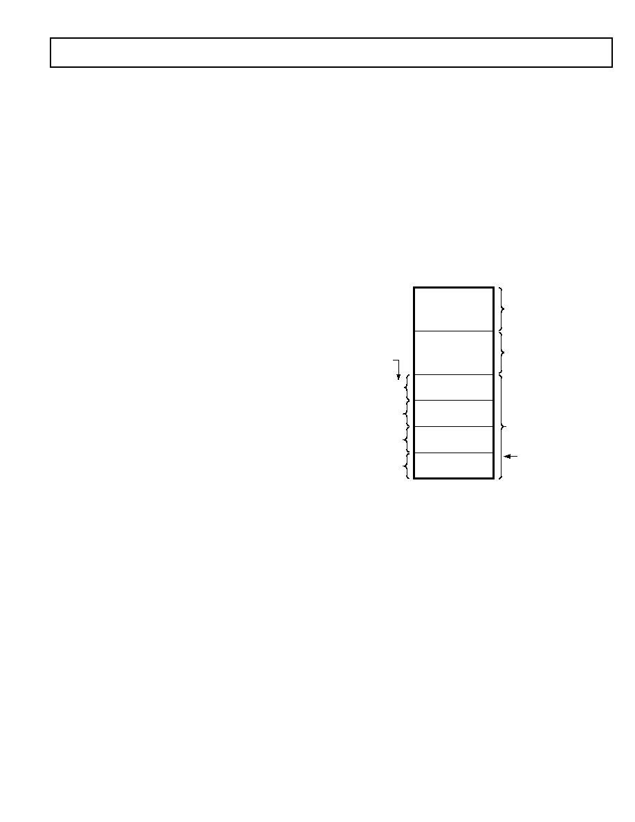
The lower 128 bytes of internal data memory are mapped as
shown in Figure 23. The lowest 32 bytes are grouped into four
banks of eight registers addressed as R0 to R7. The next 16 bytes
(128 bits), locations 20H to 2FH above the register banks, form
a block of directly addressable bit locations at Bit Addresses
00H to 7FH. The stack can be located anywhere in the internal
memory address space, and the stack depth can be expanded up
to 2048 bytes.
Reset initializes the stack pointer to location 07H and incre-
ments it once before loading the stack to start from location
08H, which is also the first register (R0) of register bank 1. Thus,
if the user needs to use more than one register bank, the stack
pointer should be initialized to an area of RAM not used for
data storage.
11
10
01
00
07H
0FH
17H
1FH
2FH
7FH
00H
08H
10H
18H
20H
RESET VALUE OF
STACK POINTER
30H
FOUR BANKS OF EIGHT
REGISTERS
R0 TO R7
BIT-ADDRESSABLE
(BIT ADDRESSES)
GENERAL-PURPOSE
AREA
BANKS
SELECTED
VIA
BITS IN PSW
03260-0-021
Figure 23. Lower 128 Bytes of Internal Data Memory
The parts contain 2048 bytes of internal XRAM, 1792 bytes of
which can be configured to an extended 11-bit stack pointer.
By default, the stack operates exactly like an 8052 in that it rolls
over from FFH to 00H in the general-purpose RAM. On the
parts, however, it is possible (by setting CFG841.7 or CFG842.7)
to enable the 11-bit extended stack pointer. In this case, the
stack rolls over from FFH in RAM to 0100H in XRAM.
The 11-bit stack pointer is visible in the SP and SPH SFRs. The
SP SFR is located at 81H as with a standard 8052. The SPH SFR
is located at B7H. The 3 LSBs of this SFR contain the 3 extra bits
necessary to extend the 8-bit stack pointer into an 11-bit stack
pointer.
相关PDF资料 |
PDF描述 |
|---|---|
| VI-BTF-IW | CONVERTER MOD DC/DC 72V 100W |
| VI-BT4-IX | CONVERTER MOD DC/DC 48V 75W |
| ADUC7020BCPZ62-RL7 | IC MCU 12BIT 1MSPS UART 40-LFCSP |
| ADUC7020BCPZ62IRL7 | IC MCU 12BIT 1MSPS I2C 40-LFCSP |
| ADUC7032BSTZ-88-RL | IC MCU 96K FLASH DUAL 48LQFP |
相关代理商/技术参数 |
参数描述 |
|---|---|
| ADUC843BS62-3 | 制造商:Analog Devices 功能描述:MCU 8-Bit ADuC8xx 8052 CISC 62KB Flash 3V 52-Pin MQFP |
| ADUC843BS62-5 | 制造商:Analog Devices 功能描述:IC MICROCONTROLLER |
| ADUC843BSZ62-3 | 功能描述:IC ADC 12BIT W/FLASH MCU 52-MQFP RoHS:是 类别:集成电路 (IC) >> 嵌入式 - 微控制器, 系列:MicroConverter® ADuC8xx 标准包装:250 系列:LPC11Uxx 核心处理器:ARM? Cortex?-M0 芯体尺寸:32-位 速度:50MHz 连通性:I²C,Microwire,SPI,SSI,SSP,UART/USART,USB 外围设备:欠压检测/复位,POR,WDT 输入/输出数:40 程序存储器容量:96KB(96K x 8) 程序存储器类型:闪存 EEPROM 大小:4K x 8 RAM 容量:10K x 8 电压 - 电源 (Vcc/Vdd):1.8 V ~ 3.6 V 数据转换器:A/D 8x10b 振荡器型:内部 工作温度:-40°C ~ 85°C 封装/外壳:48-LQFP 包装:托盘 其它名称:568-9587 |
| ADUC843BSZ62-5 | 功能描述:IC ADC 12BIT W/FLASH MCU 52-MQFP RoHS:是 类别:集成电路 (IC) >> 嵌入式 - 微控制器, 系列:MicroConverter® ADuC8xx 标准包装:60 系列:PSOC® 3 CY8C38xx 核心处理器:8051 芯体尺寸:8-位 速度:67MHz 连通性:EBI/EMI,I²C,LIN,SPI,UART/USART 外围设备:电容感应,DMA,LCD,POR,PWM,WDT 输入/输出数:25 程序存储器容量:64KB(64K x 8) 程序存储器类型:闪存 EEPROM 大小:2K x 8 RAM 容量:8K x 8 电压 - 电源 (Vcc/Vdd):1.71 V ~ 5.5 V 数据转换器:A/D 2x20b,D/A 4x8b 振荡器型:内部 工作温度:-40°C ~ 85°C 封装/外壳:48-VFQFN 裸露焊盘 包装:托盘 |
| ADUC844 | 制造商:AD 制造商全称:Analog Devices 功能描述:MicroConverter, Dual 16-Bit/24-Bit ADCs with Embedded 62kB FLASH MCU |
发布紧急采购,3分钟左右您将得到回复。