- 您现在的位置:买卖IC网 > PDF目录11199 > ADUC845BSZ8-5-RL (Analog Devices Inc)IC FLASH MCU W/24BIT ADC 56-CSP PDF资料下载
参数资料
| 型号: | ADUC845BSZ8-5-RL |
| 厂商: | Analog Devices Inc |
| 文件页数: | 72/108页 |
| 文件大小: | 0K |
| 描述: | IC FLASH MCU W/24BIT ADC 56-CSP |
| 标准包装: | 1 |
| 系列: | MicroConverter® ADuC8xx |
| 核心处理器: | 8052 |
| 芯体尺寸: | 8-位 |
| 速度: | 12.58MHz |
| 连通性: | I²C,SPI,UART/USART |
| 外围设备: | POR,PSM,PWM,温度传感器,WDT |
| 输入/输出数: | 34 |
| 程序存储器容量: | 8KB(8K x 8) |
| 程序存储器类型: | 闪存 |
| EEPROM 大小: | 4K x 8 |
| RAM 容量: | 2.25K x 8 |
| 电压 - 电源 (Vcc/Vdd): | 4.75 V ~ 5.25 V |
| 数据转换器: | A/D 10x24b; D/A 1x12b,2x16b |
| 振荡器型: | 内部 |
| 工作温度: | -40°C ~ 125°C |
| 封装/外壳: | 52-QFP |
| 包装: | 标准包装 |
| 其它名称: | ADUC845BSZ8-5-RLDKR |
第1页第2页第3页第4页第5页第6页第7页第8页第9页第10页第11页第12页第13页第14页第15页第16页第17页第18页第19页第20页第21页第22页第23页第24页第25页第26页第27页第28页第29页第30页第31页第32页第33页第34页第35页第36页第37页第38页第39页第40页第41页第42页第43页第44页第45页第46页第47页第48页第49页第50页第51页第52页第53页第54页第55页第56页第57页第58页第59页第60页第61页第62页第63页第64页第65页第66页第67页第68页第69页第70页第71页当前第72页第73页第74页第75页第76页第77页第78页第79页第80页第81页第82页第83页第84页第85页第86页第87页第88页第89页第90页第91页第92页第93页第94页第95页第96页第97页第98页第99页第100页第101页第102页第103页第104页第105页第106页第107页第108页
ADuC845/ADuC847/ADuC848
Data Sheet
Rev. C | Page 66 of 108
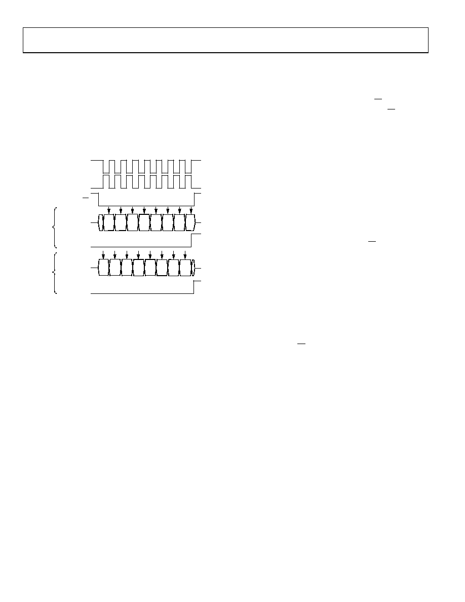
USING THE SPI INTERFACE
Depending on the configuration of the bits in the SPICON
SFR shown in Table 41, the SPI interface transmits or receives
data in a number of possible modes. Figure 46 shows all
possible ADuC845/ADuC847/ADuC848 SPI configurations
and the timing relationships and synchronization among the
signals involved. Also shown in this figure is the SPI interrupt
bit (ISPI) and how it is triggered at the end of each byte-wide
communication.
SCLOCK
(CPOL = 1)
SCLOCK
(CPOL = 0)
(CPHA = 1)
(CPHA = 0)
SAMPLE INPUT
ISPI FLAG
DATA OUTPUT
ISPI FLAG
SAMPLE INPUT
DATA OUTPUT
?
MSB BIT 6 BIT 5 BIT 4 BIT 3 BIT 2 BIT 1 LSB
SS
04741-046
Figure 46. SPI Timing, All Modes
SPI Interface—Master Mode
In master mode, the SCLOCK pin is always an output and
generates a burst of eight clocks whenever user code writes to
the SPIDAT register. The SCLOCK bit rate is determined by
SPR0 and SPR1 in SPICON. Also note that the SS pin is not
used in master mode. If the parts need to assert the SS pin on an
external slave device, a port digital output pin should be used.
In master mode, a byte transmission or reception is initiated by
a byte write to SPIDAT. The hardware automatically generates
eight clock periods via the SCLOCK pin, and the data is
transmitted via MOSI. With each SCLOCK period, a data bit is
also sampled via MISO. After eight clocks, the transmitted byte
is completely transmitted (via MOSI), and the input byte (if
required) is waiting in the input shift register (after being
received via MISO). The ISPI flag is set automatically, and an
interrupt occurs if enabled. The value in the input shift register
is latched into SPIDAT.
SPI Interface—Slave Mode
In slave mode, the SCLOCK is an input. The SS pin must also
be driven low externally during the byte communication. Trans-
mission is also initiated by a write to SPIDAT. In slave mode, a
data bit is transmitted via MISO, and a data bit is received via
MOSI through each input SCLOCK period. After eight clocks,
the transmitted byte is completely transmitted, and the input
byte is waiting in the input shift register. The ISPI flag is set
automatically, and an interrupt occurs, if enabled. The value in
the shift register is latched into SPIDAT only when the trans-
mission/reception of a byte has been completed. The end of
transmission occurs after the eighth clock has been received if
CPHA = 1, or when SS returns high if CPHA = 0.
相关PDF资料 |
PDF描述 |
|---|---|
| MC74HCT4051ADG | ANALOG MULTIPLEXERS/DEMU SOIC16 |
| ADUC7036DCPZ | IC MCU 96K FLASH DUAL 48LFCSP |
| MC74HC4051ADTR2G | IC MUX/DEMUX 8X1 16TSSOP |
| ADUC7036BCPZ | IC MCU FLASH 96K ANLGI/O 48LFCSP |
| ATSAM3X4EA-AU | IC MCU 2X128KB CORTEX-M3 144-QFP |
相关代理商/技术参数 |
参数描述 |
|---|---|
| ADUC846 | 制造商:AD 制造商全称:Analog Devices 功能描述:MicroConverter, Dual 16-Bit ADCs with Embedded 62kB FLASH MCU |
| ADUC846BCP32-3 | 制造商:AD 制造商全称:Analog Devices 功能描述:MicroConverter, Dual 16-Bit ADCs with Embedded 62kB FLASH MCU |
| ADUC846BCP32-5 | 制造商:AD 制造商全称:Analog Devices 功能描述:MicroConverter, Dual 16-Bit ADCs with Embedded 62kB FLASH MCU |
| ADUC846BCP62-3 | 制造商:AD 制造商全称:Analog Devices 功能描述:MicroConverter, Dual 16-Bit ADCs with Embedded 62kB FLASH MCU |
| ADUC846BCP62-5 | 制造商:AD 制造商全称:Analog Devices 功能描述:MicroConverter, Dual 16-Bit ADCs with Embedded 62kB FLASH MCU |
发布紧急采购,3分钟左右您将得到回复。