- 您现在的位置:买卖IC网 > PDF目录11201 > ADUC847BCPZ8-3 (Analog Devices Inc)IC MCU FLASH W/24BIT ADC 56-CSP PDF资料下载
参数资料
| 型号: | ADUC847BCPZ8-3 |
| 厂商: | Analog Devices Inc |
| 文件页数: | 36/108页 |
| 文件大小: | 0K |
| 描述: | IC MCU FLASH W/24BIT ADC 56-CSP |
| 标准包装: | 1 |
| 系列: | MicroConverter® ADuC8xx |
| 核心处理器: | 8052 |
| 芯体尺寸: | 8-位 |
| 速度: | 12.58MHz |
| 连通性: | I²C,SPI,UART/USART |
| 外围设备: | POR,PSM,PWM,温度传感器,WDT |
| 输入/输出数: | 34 |
| 程序存储器容量: | 8KB(8K x 8) |
| 程序存储器类型: | 闪存 |
| EEPROM 大小: | 4K x 8 |
| RAM 容量: | 2.25K x 8 |
| 电压 - 电源 (Vcc/Vdd): | 2.7 V ~ 3.6 V |
| 数据转换器: | A/D 10x24b; D/A 1x12b,2x16b |
| 振荡器型: | 内部 |
| 工作温度: | -40°C ~ 85°C |
| 封装/外壳: | 56-VFQFN 裸露焊盘,CSP |
| 包装: | 托盘 |
| 配用: | EVAL-ADUC847QSZ-ND - KIT DEV QUICK START FOR ADUC847 |
第1页第2页第3页第4页第5页第6页第7页第8页第9页第10页第11页第12页第13页第14页第15页第16页第17页第18页第19页第20页第21页第22页第23页第24页第25页第26页第27页第28页第29页第30页第31页第32页第33页第34页第35页当前第36页第37页第38页第39页第40页第41页第42页第43页第44页第45页第46页第47页第48页第49页第50页第51页第52页第53页第54页第55页第56页第57页第58页第59页第60页第61页第62页第63页第64页第65页第66页第67页第68页第69页第70页第71页第72页第73页第74页第75页第76页第77页第78页第79页第80页第81页第82页第83页第84页第85页第86页第87页第88页第89页第90页第91页第92页第93页第94页第95页第96页第97页第98页第99页第100页第101页第102页第103页第104页第105页第106页第107页第108页
Data Sheet
ADuC845/ADuC847/ADuC848
Rev. C | Page 33 of 108
of the input voltage on the analog input channel can be taken.
When the resulting voltage measured is full scale, the transducer
has gone open circuit. When the voltage measured is 0 V, this
indicates that the transducer has gone short circuit. The current
sources work over the normal absolute input voltage range
specifications.
REFERENCE DETECT CIRCUIT
The main and auxiliary (ADuC845 only) ADCs can be config-
ured to allow the use of the internal band gap reference or an
external reference that is applied to the REFIN± pins by means
of the XREF0/1 bit in the Control Registers AD0CON2 and
AD1CON (ADuC845 only). A reference detection circuit is
provided to detect whether a valid voltage is applied to the
REFIN± pins. This feature arose in connection with strain-gage
sensors in weigh scales where the reference and signal are
provided via a cable from the remote sensor. It is desirable to
detect whether the cable is disconnected. If either of the pins is
floating or if the applied voltage is below a specified threshold, a
flag (NOXREF) is set in the ADC status register (ADCSTAT),
conversion results are clamped, and calibration registers are not
updated if a calibration is in progress.
Note that the reference detect does not look at REFIN2± pins.
If, during either an offset or gain calibration, the NOEXREF bit
becomes active, indicating an incorrect VREF, updating the relevant
calibration register is inhibited to avoid loading incorrect data
into these registers, and the appropriate bits in ADCSTAT (ERR0
or ERR1) are set. If the user needs to verify that a valid reference
is in place every time a calibration is performed, the status of
the ERR0 and ERR1 bits should be checked at the end of every
calibration cycle.
SINC FILTER REGISTER (SF)
The number entered into the SF register sets the decimation
The range of operation of the SF word depends on whether
ADC chop is on or off. With chop disabled, the minimum SF
word is 3 and the maximum is 255. This gives an ADC through-
put rate from 16.06 Hz to 1.365 kHz. With chop enabled, the
minimum SF word is 13 (all values lower than 13 are clamped
to 13) and the maximum is 255. This gives an ADC throughput
rate of 5.4 Hz to 105 Hz. See the fADC equation in the ADC
description preceding section.
An additional feature of the Sinc3 filter is a second notch filter
positioned in the frequency response at 60 Hz. This gives
simultaneous 60 Hz rejection to whatever notch is defined by
the SF filter. This 60 Hz filter is enabled via the REJ60 bit in the
ADCMODE register (ADCMODE.6). The notch is valid only
for SF words ≥ 68; otherwise, ADC errors occur, and, the notch
is best used with an SF word of 82d giving simultaneous 50 Hz
and 60 Hz rejection. This function is useful only with an ADC
clock (modulator rate) of 32.768 kHz. During calibration, the
current (user-written) value of the SF register is used.
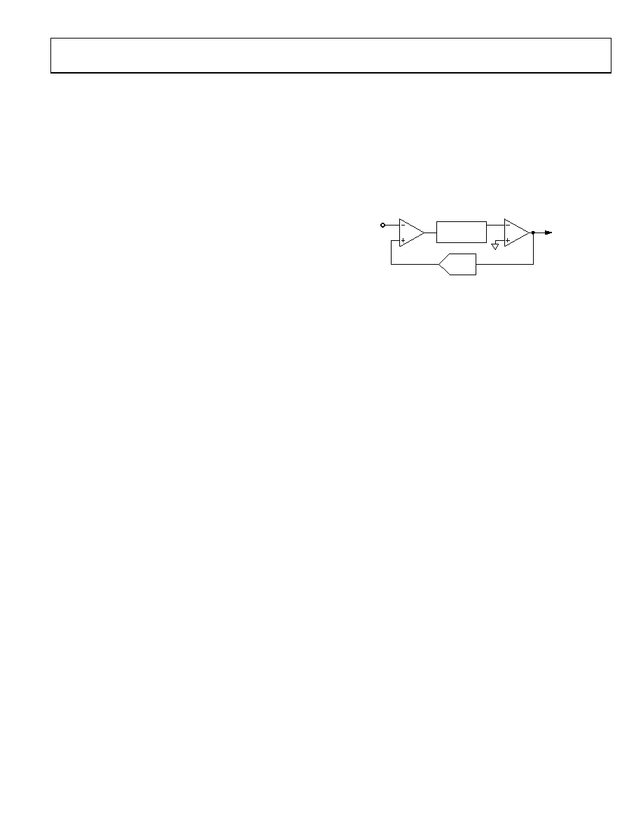
Σ- MODULATOR
A Σ- ADC usually consists of two main blocks, an analog
modulator, and a digital filter. For the ADuC845/ADuC847/
ADuC848, the analog modulator consists of a difference
amplifier, an integrator block, a comparator, and a feedback
DAC as shown in Figure 16.
INTEGRATOR
COMPARATOR
DIFFERENCE
AMP
ANALOG
INPUT
HIGH
FREQUENCY
BIT STREAM
TO DIGITAL
FILTER
DAC
04741-016
Figure 16. Σ- Modulator Simplified Block Diagram
In operation, the analog signal is fed to the difference amplifier
along with the output from the feedback DAC. The difference
between these two signals is integrated and fed to the comparator.
The output from the comparator provides the input to the feed-
back DAC so the system functions as a negative feedback loop
that tries to minimize the difference signal. The digital data that
represents the analog input voltage is contained in the duty cycle of
the pulse train appearing at the output of the comparator. This duty
cycle data can be recovered as a data-word by using a subsequent
digital filter stage. The sampling frequency of the modulator
loop is many times higher than the bandwidth of the input signal.
The integrator in the modulator shapes the quantization noise
(that results from the analog-to-digital conversion) so that the
noise is pushed toward one-half of the modulator frequency.
DIGITAL FILTER
The output of the ∑- modulator feeds directly into the digital
filter. The digital filter then band-limits the response to a
frequency significantly lower than one-half of the modulator
frequency. In this manner, the 1-bit output of the comparator is
translated into a band-limited, low noise output from the part.
The ADuC845/ADuC847/ADuC848 filter is a low-pass, Sinc3
or [(SINx)/x]3 filter whose primary function is to remove the
quantization noise introduced at the modulator. The cutoff
frequency and decimated output data rate of the filter are
programmable via the SF (Sinc filter) SFR as listed in Table 28
and Table 29.
Figure 22, Figure 23, Figure 24, and Figure 25 show the frequency
response of the ADC, yielding an overall output rate of 16.6 Hz
with chop enabled and 50 Hz with chop disabled. Also detailed
in these plots is the effect of the fixed 60 Hz drop-in notch filter
(REJ60 bit, ADCMODE.6). This fixed filter can be enabled or
disabled by setting or clearing the REJ60 bit in the ADCMODE
register (ADCMODE.6). This 60 Hz drop-in notch filter can be
相关PDF资料 |
PDF描述 |
|---|---|
| VE-BTR-IW | CONVERTER MOD DC/DC 7.5V 100W |
| VE-BTM-IX | CONVERTER MOD DC/DC 10V 75W |
| VE-BT1-IX | CONVERTER MOD DC/DC 12V 75W |
| VE-B5N-IX | CONVERTER MOD DC/DC 18.5V 75W |
| VE-B5N-IW | CONVERTER MOD DC/DC 18.5V 100W |
相关代理商/技术参数 |
参数描述 |
|---|---|
| ADUC847BCPZ8-5 | 功能描述:IC MCU FLASH W/24BIT ADC 56-CSP RoHS:是 类别:集成电路 (IC) >> 嵌入式 - 微控制器, 系列:MicroConverter® ADuC8xx 标准包装:38 系列:Encore!® XP® 核心处理器:eZ8 芯体尺寸:8-位 速度:5MHz 连通性:IrDA,UART/USART 外围设备:欠压检测/复位,LED,POR,PWM,WDT 输入/输出数:16 程序存储器容量:4KB(4K x 8) 程序存储器类型:闪存 EEPROM 大小:- RAM 容量:1K x 8 电压 - 电源 (Vcc/Vdd):2.7 V ~ 3.6 V 数据转换器:- 振荡器型:内部 工作温度:-40°C ~ 105°C 封装/外壳:20-SOIC(0.295",7.50mm 宽) 包装:管件 其它名称:269-4116Z8F0413SH005EG-ND |
| ADUC847BS32-3 | 制造商:Analog Devices 功能描述:MCU 8-Bit ADuC8xx 8052 CISC 62KB Flash 3.3V/5V 52-Pin MQFP 制造商:Rochester Electronics LLC 功能描述:8BIT CISC 62KB FLASH 12.85MHZ 3.3V 52MQFP - Bulk |
| ADUC847BS32-5 | 制造商:Analog Devices 功能描述:MCU 8-Bit ADuC8xx 8052 CISC 62KB Flash 3.3V/5V 52-Pin MQFP 制造商:Rochester Electronics LLC 功能描述: |
| ADUC847BS62-3 | 制造商:Analog Devices 功能描述:MCU 8-Bit ADuC8xx 8052 CISC 62KB Flash 3.3V/5V 52-Pin MQFP 制造商:Rochester Electronics LLC 功能描述:8BIT CISC 62KB FLASH 12.85MHZ 3.3V 52MQFP - Bulk |
| ADUC847BS62-5 | 制造商:Analog Devices 功能描述:MCU 8-bit ADuC8xx 8052 CISC 62KB Flash 3.3V/5V 52-Pin MQFP 制造商:Analog Devices 功能描述:IC MICROCONTROLLER |
发布紧急采购,3分钟左右您将得到回复。