- 您现在的位置:买卖IC网 > PDF目录11197 > ADUC848BCPZ62-3 (Analog Devices Inc)IC MCU FLASH W/16BIT ADC 56-CSP PDF资料下载
参数资料
| 型号: | ADUC848BCPZ62-3 |
| 厂商: | Analog Devices Inc |
| 文件页数: | 95/108页 |
| 文件大小: | 0K |
| 描述: | IC MCU FLASH W/16BIT ADC 56-CSP |
| 标准包装: | 1 |
| 系列: | MicroConverter® ADuC8xx |
| 核心处理器: | 8052 |
| 芯体尺寸: | 8-位 |
| 速度: | 12.58MHz |
| 连通性: | I²C,SPI,UART/USART |
| 外围设备: | POR,PSM,PWM,温度传感器,WDT |
| 输入/输出数: | 34 |
| 程序存储器容量: | 62KB(62K x 8) |
| 程序存储器类型: | 闪存 |
| EEPROM 大小: | 4K x 8 |
| RAM 容量: | 2.25K x 8 |
| 电压 - 电源 (Vcc/Vdd): | 2.7 V ~ 3.6 V |
| 数据转换器: | A/D 10x16b; D/A 1x12b,2x16b |
| 振荡器型: | 内部 |
| 工作温度: | -40°C ~ 85°C |
| 封装/外壳: | 56-VFQFN 裸露焊盘,CSP |
| 包装: | 托盘 |
第1页第2页第3页第4页第5页第6页第7页第8页第9页第10页第11页第12页第13页第14页第15页第16页第17页第18页第19页第20页第21页第22页第23页第24页第25页第26页第27页第28页第29页第30页第31页第32页第33页第34页第35页第36页第37页第38页第39页第40页第41页第42页第43页第44页第45页第46页第47页第48页第49页第50页第51页第52页第53页第54页第55页第56页第57页第58页第59页第60页第61页第62页第63页第64页第65页第66页第67页第68页第69页第70页第71页第72页第73页第74页第75页第76页第77页第78页第79页第80页第81页第82页第83页第84页第85页第86页第87页第88页第89页第90页第91页第92页第93页第94页当前第95页第96页第97页第98页第99页第100页第101页第102页第103页第104页第105页第106页第107页第108页
Data Sheet
ADuC845/ADuC847/ADuC848
Rev. C | Page 87 of 108
HARDWARE DESIGN CONSIDERATIONS
This section outlines some of the key hardware design
considerations that must be addressed when integrating the
ADuC845/ADuC847/ADuC848 into any hardware system.
EXTERNAL MEMORY INTERFACE
In addition to their internal program and data memories, the
parts can access up to 16 Mbytes of external data memory
(SRAM). No external program memory access is available.
To begin executing code, tie the EA (external access) pin high.
program execution starts at Address 0 in the internal 62-kbyte
Flash/EE code space. When executing from internal code space,
accesses to the program space above F7FFH (62 kbytes) are read
as NOP instructions.
Note that a second very important function of the EA pin is
described in the Single-Pin Emulation Mode section under the
Figure 62 shows a hardware configuration for accessing up to
64 kbytes of external data memory. This interface is standard to
any 8051-compatible MCU.
LATCH
SRAM
OE
A8–A15
A0–A7
D0–D7
(DATA)
ADuC845/
ADuC847/
ADuC848
RD
P2
ALE
P0
WE
WR
04741-059
Figure 62. External Data Memory Interface (64-kbyte Address Space)
If access to more than 64 kbytes of RAM is desired, a feature
unique to the MicroConverter allows addressing up to 16 Mbytes
of external RAM simply by adding another latch as shown in
LATCH
P2
ALE
P0
LATCH
SRAM
A8–A15
A0–A7
D0–D7
(DATA)
A16–A23
OE
RD
WE
WR
ADuC845/
ADuC847/
ADuC848
04741-060
Figure 63. External Data Memory Interface (16-Mbtye Address Space)
In either implementation, Port 0 (P0) serves as a multiplexed
address/data bus. It emits the low byte of the data pointer (DPL)
as an address, which is latched by ALE prior to data being placed
on the bus by the parts (write operation) or the external data
memory (read operation). Port 2 (P2) provides the data pointer
page byte (DPP) to be latched by ALE, followed by the data
pointer high byte (DPH). If no latch is connected to P2, DPP is
ignored by the SRAM, and the 8051 standard of 64-kbyte external
data memory access is maintained.
The following example shows the code used to write data to
external data memory.
MOV DPP, #10h ;Set addr to 100000h
MOV DPH, #00h
MOV DPL, #00h
MOV A,
#'B' ;Write Char ‘B’ (42h)
MOVX @DPTR,A
;Move to DPP:DPH:DPL addr
POWER SUPPLIES
The parts’ operational power supply voltage range is 2.7 V to
5.25 V. Although the guaranteed data sheet specifications are
given only for power supplies within 2.7 V to 3.6 V and 4.75 V
to 5.25 V (±5% of the nominal 5 V level), the chip functions
equally well at any power supply level between 2.7 V and 5.25 V.
Separate analog and digital power supply pins (AVDD and DVDD,
respectively) allow AVDD to be kept relatively free of the noisy
digital signals often present on a system DVDD line. In this mode,
the part can also operate with split supplies, that is, using different
voltage supply levels for each supply. For example, the system
can be designed to operate with a DVDD voltage level of 3 V and
the AVDD level can be at 5 V, or vice versa, if required. A typical
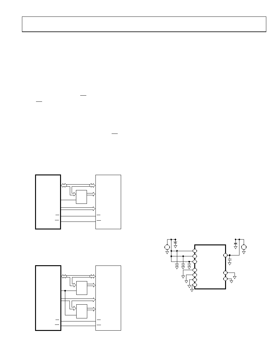
split-supply configuration is shown in Figure 64.
DIGITAL SUPPLY
ANALOG SUPPLY
DVDD
AGND
AVDD
DGND
–
+
–
+
0.1
F
0.1
F
10
F
10
F
ADuC845/
ADuC847/
ADuC848
04741-061
6
5
4
22
36
51
50
38
37
23
Figure 64. External Dual-Supply Connections
(56-Lead LFCSP Pin Numbering)
As an alternative to providing two separate power supplies,
AVDD can be kept quiet by placing a small series resistor and/or
ferrite bead between it and DVDD, and then decoupling AVDD
separately to ground. An example of this configuration is shown
in Figure 65. In this configuration, other analog circuitry (such
相关PDF资料 |
PDF描述 |
|---|---|
| ADUC847BCPZ62-3 | IC MCU FLASH 24BIT ADC 56LFCSP |
| AT91SAM7XC256B-CU | MCU ARM 256K HS FLASH 100-TFBGA |
| EP7312M-CBZ | IC ARM720T MCU 74MHZ 256-PBGA |
| EP9301-IQZ | IC ARM920T MCU 166MHZ 208-LQFP |
| AT91SAM7X256C-CU | IC MCU 32BIT 256KB FLSH 100TFBGA |
相关代理商/技术参数 |
参数描述 |
|---|---|
| ADUC848BCPZ62-5 | 功能描述:IC MCU FLASH W/16BIT ADC 56LFCSP RoHS:是 类别:集成电路 (IC) >> 嵌入式 - 微控制器, 系列:MicroConverter® ADuC8xx 标准包装:38 系列:Encore!® XP® 核心处理器:eZ8 芯体尺寸:8-位 速度:5MHz 连通性:IrDA,UART/USART 外围设备:欠压检测/复位,LED,POR,PWM,WDT 输入/输出数:16 程序存储器容量:4KB(4K x 8) 程序存储器类型:闪存 EEPROM 大小:- RAM 容量:1K x 8 电压 - 电源 (Vcc/Vdd):2.7 V ~ 3.6 V 数据转换器:- 振荡器型:内部 工作温度:-40°C ~ 105°C 封装/外壳:20-SOIC(0.295",7.50mm 宽) 包装:管件 其它名称:269-4116Z8F0413SH005EG-ND |
| ADUC848BCPZ8-3 | 功能描述:IC MCU FLASH W/16BIT ADC 56-CSP RoHS:是 类别:集成电路 (IC) >> 嵌入式 - 微控制器, 系列:MicroConverter® ADuC8xx 标准包装:38 系列:Encore!® XP® 核心处理器:eZ8 芯体尺寸:8-位 速度:5MHz 连通性:IrDA,UART/USART 外围设备:欠压检测/复位,LED,POR,PWM,WDT 输入/输出数:16 程序存储器容量:4KB(4K x 8) 程序存储器类型:闪存 EEPROM 大小:- RAM 容量:1K x 8 电压 - 电源 (Vcc/Vdd):2.7 V ~ 3.6 V 数据转换器:- 振荡器型:内部 工作温度:-40°C ~ 105°C 封装/外壳:20-SOIC(0.295",7.50mm 宽) 包装:管件 其它名称:269-4116Z8F0413SH005EG-ND |
| ADUC848BCPZ8-5 | 功能描述:IC MCU FLASH W/16BIT ADC 56-CSP RoHS:是 类别:集成电路 (IC) >> 嵌入式 - 微控制器, 系列:MicroConverter® ADuC8xx 标准包装:38 系列:Encore!® XP® 核心处理器:eZ8 芯体尺寸:8-位 速度:5MHz 连通性:IrDA,UART/USART 外围设备:欠压检测/复位,LED,POR,PWM,WDT 输入/输出数:16 程序存储器容量:4KB(4K x 8) 程序存储器类型:闪存 EEPROM 大小:- RAM 容量:1K x 8 电压 - 电源 (Vcc/Vdd):2.7 V ~ 3.6 V 数据转换器:- 振荡器型:内部 工作温度:-40°C ~ 105°C 封装/外壳:20-SOIC(0.295",7.50mm 宽) 包装:管件 其它名称:269-4116Z8F0413SH005EG-ND |
| ADUC848BS32-3 | 制造商:AD 制造商全称:Analog Devices 功能描述:MicroConverter Multichannel 24-/16-Bit ADCs with Embedded 62 kB Flash and Single-Cycle MCU |
| ADUC848BS32-5 | 制造商:Analog Devices 功能描述:IC MICROCONTROLLER |
发布紧急采购,3分钟左右您将得到回复。