- 您现在的位置:买卖IC网 > PDF目录21410 > ADUM4223CRWZ-RL (Analog Devices Inc)IC 5KV ISO HALF BR DRVR 16SOIC PDF资料下载
参数资料
| 型号: | ADUM4223CRWZ-RL |
| 厂商: | Analog Devices Inc |
| 文件页数: | 15/20页 |
| 文件大小: | 0K |
| 描述: | IC 5KV ISO HALF BR DRVR 16SOIC |
| 标准包装: | 1,000 |
| 系列: | * |
�� ��
��
��Data� Sheet�
�APPLICATIONS� INFORMATION�
�PC� BOARD� LAYOUT�
�The� ADuM3223� /� ADuM4223� digital� isolators� require� no� exter-�
�nal� interface� circuitry� for� the� logic� interfaces.� Power� supply�
�bypassing� is� required� at� the� input� and� output� supply� pins,� as�
�shown� in� Figure� 19.� Use� a� small� ceramic� capacitor� with� a� value�
�between� 0.01� μF� and� 0.1� μF� to� provide� a� good� high� frequency�
�bypass.� On� the� output� power� supply� pin,� V� DDA� or� V� DDB� ,� it� is�
�recommended� to� also� add� a� 10� μF� capacitor� to� provide� the�
�charge� required� to� drive� the� gate� capacitance� at� the� ADuM3223� /�
�ADuM4223� outputs.� On� the� output� supply� pin,� the� bypass�
�capacitor� use� of� vias� should� be� avoided� or� multiple� vias� should�
�be� employed� to� reduce� the� inductance� in� the� bypassing.� The�
�total� lead� length� between� both� ends� of� the� smaller� capacitor� and�
�the� input� or� output� power� supply� pin� should� not� exceed� 5� mm.�
�ADuM3223/ADuM4223�
�Channel-to-channel� matching� refers� to� the� maximum� amount�
�that� the� propagation� delay� differs� between� channels� within� a�
�single� ADuM3223� /� ADuM4223� component.�
�Propagation� delay� skew� refers� to� the� maximum� amount� that�
�the� propagation� delay� differs� between� multiple� ADuM3223� /�
�ADuM4223� components� operating� under� the� same� conditions.�
�THERMAL� LIMITATIONS� AND� SWITCH� LOAD�
�CHARACTERISTICS�
�For� isolated� gate� drivers,� the� necessary� separation� between� the�
�input� and� output� circuits� prevents� the� use� of� a� single� thermal�
�pad� beneath� the� part,� and� heat� is,� therefore,� dissipated� mainly�
�through� the� package� pins.�
�Package� thermal� dissipation� limits� the� performance� of� switching�
�frequency� vs.� output� load,� as� illustrated� in� Figure� 7� and� Figure� 8�
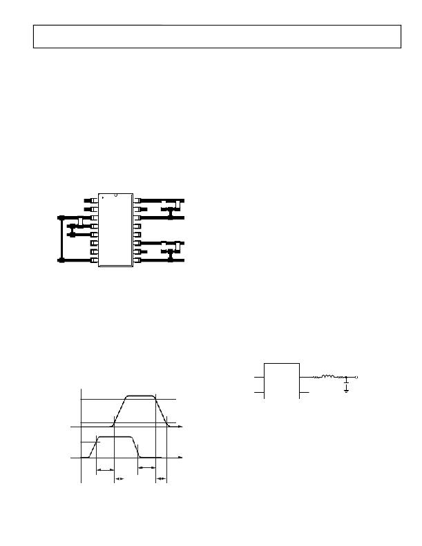
�V� DD1�
�GND� 1�
�DISABLE�
�V� DD1�
�V� IA�
�V� IB�
�NC�
�NC�
�NC�
�NC�
�V� OA�
�V� OB�
�V� DDA�
�GND� A�
�V� DDB�
�GND� B�
�for� the� maximum� load� capacitance� that� can� be� driven� with� a� 1� Ω�
�series� gate� resistance� for� different� values� of� output� voltage.� For�
�example,� this� curve� shows� that� a� typical� ADuM3223� can� drive� a�
�large� MOSFET� with� 140� nC� gate� charge� at� 8� V� output� (which� is�
�equivalent� to� a� 17� nF� load)� up� to� a� frequency� of� about� 300� kHz.�
�Each� of� the� ADuM3223� /� ADuM4223� isolator� outputs� has� a� thermal�
�shutdown� protection� function,� which� sets� an� output� to� a� logic�
�low� when� the� rising� junction� temperature� typically� reaches�
�Figure� 19.� Recommended� PCB� Layout�
�PROPAGATION� DELAY-RELATED� PARAMETERS�
�Propagation� delay� is� a� parameter� that� describes� the� time� it� takes�
�a� logic� signal� to� propagate� through� a� component.� The� propagation�
�delay� to� a� logic� low� output� can� differ� from� the� propagation� delay�
�to� a� logic� high� output.� The� ADuM3223� /� ADuM4223� specify� t� DLH�
�(see� Figure� 20)� as� the� time� between� the� rising� input� high� logic�
�threshold,� V� IH� ,� to� the� output� rising� 10%� threshold.� Likewise,� the�
�falling� propagation� delay,� t� DHL� ,� is� defined� as� the� time� between�
�the� input� falling� logic� low� threshold,� V� IL� ,� and� the� output� falling�
�90%� threshold.� The� rise� and� fall� times� are� dependent� on� the�
�150°C,� and� turns� back� on� after� the� junction� temperature� falls�
�from� the� shutdown� by� approximately� 10°C.�
�OUTPUT� LOAD� CHARACTERISTICS�
�The� ADuM3223� /� ADuM4223� output� signals� depend� on� the�
�characteristics� of� the� output� load,� which� is� typically� an� N-channel�
�MOSFET.� The� driver� output� response� to� an� N-channel� MOSFET�
�load� can� be� modeled� with� a� switch� output� resistance� (R� SW� ),� an�
�inductance� due� to� the� printed� circuit� board� trace� (L� TRACE� ),� a� series�
�gate� resistor� (R� GATE� ),� and� a� gate-to-source� capacitance� (C� gs� ),� as�
�shown� in� Figure� 21.�
�loading� conditions� and� are� not� included� in� the� propagation�
�delay,� which� is� the� industry� standard� for� gate� drivers.�
�V� IA�
�ADuM3223/�
�ADuM4223�
�V� OA� R� SW�
�R� GATE�
�L� TRACE�
�C� GS�
�V� O�
�90%�
�Figure� 21.� RLC� Model� of� the� Gate� of� an� N-Channel� MOSFET�
�OUTPUT�
�R� SW� is� the� switch� resistance� of� the� internal� ADuM3223� /� ADuM4223�
�10%�
�V� IH�
�driver� output,� which� is� about� 1.1� Ω.� R� GATE� is� the� intrinsic� gate�
�resistance� of� the� MOSFET� and� any� external� series� resistance.� A�
�MOSFET� that� requires� a� 4� A� gate� driver� has� a� typical� intrinsic�
�INPUT�
�V� IL�
�t� DLH�
�t� R�
�t� DHL�
�t� F�
�gate� resistance� of� about� 1� Ω� and� a� gate-to-source� capacitance,�
�C� GS� ,� of� between� 2� nF� and� 10� nF.� L� TRACE� is� the� inductance� of� the�
�printed� circuit� board� trace,� typically� a� value� of� 5� nH� or� less� for� a�
�well-designed� layout� with� a� very� short� and� wide� connection� from�
�Figure� 20.� Propagation� Delay� Parameters�
�the� ADuM3223� /� ADuM4223� output� to� the� gate� of� the� MOSFET.�
�Rev.� D� |� Page� 15� of� 20�
�相关PDF资料 |
PDF描述 |
|---|---|
| 1879456-2 | RES 1.2 OHM 2000W 5% WW LUG |
| 3-640473-3 | CONN RCPT 3POS 20AWG .156 YELLOW |
| ADUM4223BRWZ-RL | IC 5KV ISO HALF BR DRVR 16SOIC |
| 1625949-1 | RES 11M OHM 30W 1% TF FERR |
| 3-644860-2 | CONN RCPT 2POS 18AWG MTA-156 |
相关代理商/技术参数 |
参数描述 |
|---|---|
| ADUM4223WARWZ | 功能描述:4A Gate Driver Magnetic Coupling 5000Vrms 2 Channel 16-SOIC 制造商:analog devices inc. 系列:iCoupler? 包装:管件 零件状态:有效 技术:磁耦合 通道数:2 电压 - 隔离:5000Vrms 共模瞬态抗扰度(最小值):50kV/μs 传播延迟 tpLH / tpHL(最大值):59ns,59ns 脉宽失真(最大):- 上升/下降时间(典型值):12ns,12ns 电流 - 输出高,低:- 电流 - 峰值输出:4A 电压 - 正向(Vf)(典型值):- 电流 - DC 正向(If):- 电压 - 电源:4.5 V ~ 18 V 工作温度:-40°C ~ 125°C 安装类型:表面贴装 封装/外壳:16-SOIC(0.295",7.50mm 宽) 供应商器件封装:16-SOIC 认可:CSA,UR,VDE 标准包装:47 |
| ADUM4223WARWZ-RL | 功能描述:4A Gate Driver Magnetic Coupling 5000Vrms 2 Channel 16-SOIC 制造商:analog devices inc. 系列:iCoupler? 包装:带卷(TR) 零件状态:有效 技术:磁耦合 通道数:2 电压 - 隔离:5000Vrms 共模瞬态抗扰度(最小值):50kV/μs 传播延迟 tpLH / tpHL(最大值):59ns,59ns 脉宽失真(最大):- 上升/下降时间(典型值):12ns,12ns 电流 - 输出高,低:- 电流 - 峰值输出:4A 电压 - 正向(Vf)(典型值):- 电流 - DC 正向(If):- 电压 - 电源:4.5 V ~ 18 V 工作温度:-40°C ~ 125°C 安装类型:表面贴装 封装/外壳:16-SOIC(0.295",7.50mm 宽) 供应商器件封装:16-SOIC 认可:CSA,UR,VDE 标准包装:1,000 |
| ADUM4223WBRWZ | 功能描述:4A Gate Driver Magnetic Coupling 5000Vrms 2 Channel 16-SOIC 制造商:analog devices inc. 系列:iCoupler? 包装:管件 零件状态:有效 技术:磁耦合 通道数:2 电压 - 隔离:5000Vrms 共模瞬态抗扰度(最小值):50kV/μs 传播延迟 tpLH / tpHL(最大值):54ns,54ns 脉宽失真(最大):- 上升/下降时间(典型值):12ns,12ns 电流 - 输出高,低:- 电流 - 峰值输出:4A 电压 - 正向(Vf)(典型值):- 电流 - DC 正向(If):- 电压 - 电源:7.5 V ~ 18 V 工作温度:-40°C ~ 125°C 安装类型:表面贴装 封装/外壳:16-SOIC(0.295",7.50mm 宽) 供应商器件封装:16-SOIC 认可:CSA,UR,VDE 标准包装:47 |
| ADUM4223WBRWZ-RL | 功能描述:4A Gate Driver Magnetic Coupling 5000Vrms 2 Channel 16-SOIC 制造商:analog devices inc. 系列:iCoupler? 包装:带卷(TR) 零件状态:有效 技术:磁耦合 通道数:2 电压 - 隔离:5000Vrms 共模瞬态抗扰度(最小值):50kV/μs 传播延迟 tpLH / tpHL(最大值):54ns,54ns 脉宽失真(最大):- 上升/下降时间(典型值):12ns,12ns 电流 - 输出高,低:- 电流 - 峰值输出:4A 电压 - 正向(Vf)(典型值):- 电流 - DC 正向(If):- 电压 - 电源:7.5 V ~ 18 V 工作温度:-40°C ~ 125°C 安装类型:表面贴装 封装/外壳:16-SOIC(0.295",7.50mm 宽) 供应商器件封装:16-SOIC 认可:CSA,UR,VDE 标准包装:1,000 |
| ADUM4223WCRWZ | 功能描述:4A Gate Driver Magnetic Coupling 5000Vrms 2 Channel 16-SOIC 制造商:analog devices inc. 系列:iCoupler? 包装:管件 零件状态:有效 技术:磁耦合 通道数:2 电压 - 隔离:5000Vrms 共模瞬态抗扰度(最小值):50kV/μs 传播延迟 tpLH / tpHL(最大值):54ns,54ns 脉宽失真(最大):- 上升/下降时间(典型值):12ns,12ns 电流 - 输出高,低:- 电流 - 峰值输出:4A 电压 - 正向(Vf)(典型值):- 电流 - DC 正向(If):- 电压 - 电源:11.5 V ~ 18 V 工作温度:-40°C ~ 125°C 安装类型:表面贴装 封装/外壳:16-SOIC(0.295",7.50mm 宽) 供应商器件封装:16-SOIC 认可:CSA,UR,VDE 标准包装:47 |
发布紧急采购,3分钟左右您将得到回复。