- 您现在的位置:买卖IC网 > PDF目录21462 > ADUM5230ARWZ (Analog Devices Inc)IC ISOLATOR 2CH HBRIDGE 16-SOIC PDF资料下载
参数资料
| 型号: | ADUM5230ARWZ |
| 厂商: | Analog Devices Inc |
| 文件页数: | 11/16页 |
| 文件大小: | 0K |
| 描述: | IC ISOLATOR 2CH HBRIDGE 16-SOIC |
| 其它图纸: | ADUM5230 Block Diagram |
| 标准包装: | 47 |
| 系列: | iCoupler® |
| 输入 - 1 侧/2 侧: | 2/0 |
| 通道数: | 2 |
| 电源电压: | 4.5 V ~ 5.5 V |
| 电压 - 隔离: | 2500Vrms |
| 传输延迟: | 100ns |
| 输出类型: | 逻辑 |
| 封装/外壳: | 16-SOIC(0.295",7.50mm 宽) |
| 供应商设备封装: | 16-SOIC W |
| 包装: | 管件 |
| 工作温度: | -40°C ~ 105°C |
| 产品目录页面: | 2766 (CN2011-ZH PDF) |
�� �
�
�Data� Sheet�
�PROPAGATION� DELAY-RELATED� PARAMETERS�
�Propagation� delay� is� a� parameter� that� describes� the� time� it� takes�
�a� logic� signal� to� propagate� through� a� component.� The� propagation�
�delay� to� a� logic� low� output� may� differ� from� the� propagation�
�100�
�10�
�ADuM5230�
�delay� to� a� logic� high.�
�INPUT� (V� Ix� )�
�50%�
�1�
�OUTPUT� (V� Ox� )�
�t� PLH�
�t� PHL�
�50%�
�0.1�
�0.01�
�Figure� 16.� Propagation� Delay� Parameters�
�Pulse� width� distortion� is� the� maximum� difference� between�
�these� two� propagation� delay� values� and� is� an� indication� of� how�
�0.001�
�1k�
�10k� 100k� 1M� 10M�
�MAGNETIC� FIELD� FREQUENCY� (Hz)�
�100M�
�V� =� (� ?dβ/dt� )� ∑� π� r� n� ;� n� =� 1,� 2,� …� ,� N�
�accurately� the� input� signal� timing� is� preserved.�
�Channel-to-channel� matching� refers� to� the� maximum� amount�
�the� propagation� delay� differs� between� channels� within� a� single�
�ADuM5230� component.�
�DC� CORRECTNESS� AND� MAGNETIC� FIELD� IMMUNITY�
�Positive� and� negative� logic� transitions� at� the� isolator� input�
�cause� narrow� (~1� ns)� pulses� to� be� sent� to� the� decoder� via� the�
�transformer.� The� decoder� is� bistable� and� is,� therefore,� either� set�
�or� reset� by� the� pulses,� indicating� input� logic� transitions.� In� the�
�absence� of� logic� transitions� at� the� input� for� more� than� 1� μs,� a�
�periodic� set� of� refresh� pulses� indicative� of� the� correct� input� state�
�are� sent� to� ensure� dc� correctness� at� the� output.� If� the� decoder�
�receives� no� internal� pulses� of� more� than� about� 5� μs,� the� input�
�side� is� assumed� to� be� unpowered� or� nonfunctional,� in� which�
�case� the� isolator� output� is� forced� to� a� default� state� (see� Table� 9)�
�by� the� watchdog� timer� circuit.�
�The� limitation� on� the� ADuM5230� magnetic� field� immunity� is� set�
�by� the� condition� in� which� induced� voltage� in� the� transformer�
�receiving� coil� is� sufficiently� large� to� either� falsely� set� or� reset� the�
�decoder.� The� following� analysis� defines� the� conditions� under�
�which� this� may� occur.�
�The� pulses� at� the� transformer� output� have� an� amplitude� greater�
�than� 1.0� V.� The� decoder� has� a� sensing� threshold� at� about� 0.5� V,� thus�
�establishing� a� 0.5� V� margin� in� which� induced� voltages� can� be�
�tolerated.� The� voltage� induced� across� the� receiving� coil� is� given� by�
�2�
�where:�
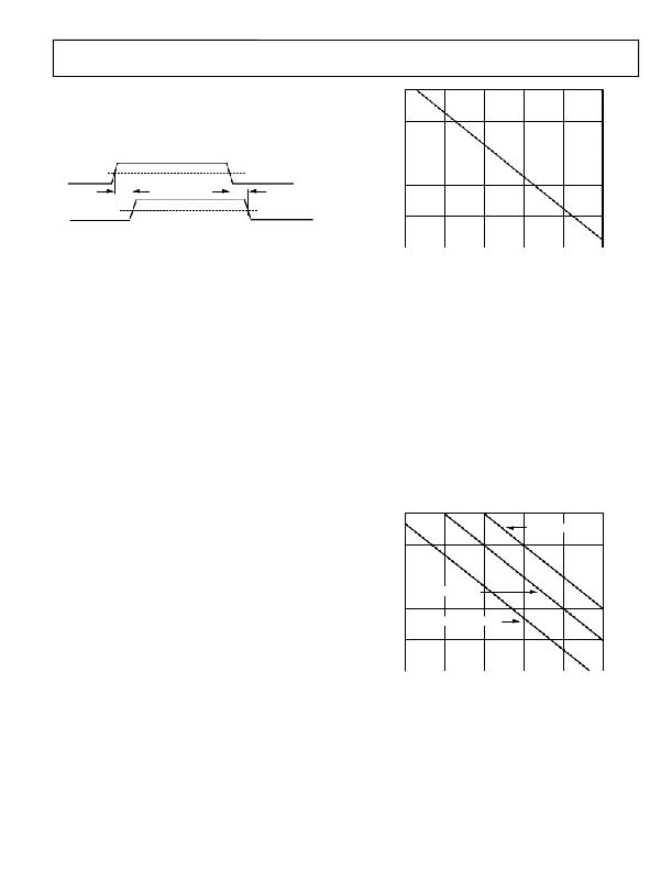
�Figure� 17.� Maximum� Allowable� External� Magnetic� Flux� Density�
�For� example,� at� a� magnetic� field� frequency� of� 1� MHz,� the� maxi-�
�mum� allowable� magnetic� field� of� 0.2� kgauss� induces� a� voltage�
�of� 0.25� V� at� the� receiving� coil.� This� is� about� 50%� of� the� sensing�
�threshold� and� does� not� cause� a� faulty� output� transition.� Similarly,�
�if� such� an� event� occurs� during� a� transmitted� pulse� (and� is� of� the�
�worst-case� polarity),� it� reduces� the� received� pulse� from� >1.0� V� to�
�0.75� V,� still� well� above� the� 0.5� V� sensing� threshold� of� the� decoder.�
�The� preceding� magnetic� flux� density� values� correspond� to� specific�
�current� magnitudes� at� given� distances� from� the� ADuM5230� trans-�
�formers.� Figure� 18� expresses� these� allowable� current� magnitudes�
�as� a� function� of� frequency� for� selected� distances.� As� shown,� the�
�ADuM5230� is� extremely� immune� and� can� be� affected� only� by�
�extremely� large� currents� operated� at� high� frequency� very� close�
�to� the� component.� For� the� 1� MHz� example� noted,� the� user� would�
�have� to� place� a� 0.5� kA� current� 5� mm� away� from� the� ADuM5230�
�to� affect� the� operation� of� the� component.�
�1000�
�DISTANCE� =� 1m�
�100�
�10�
�DISTANCE� =� 100mm�
�1�
�DISTANCE� =� 5mm�
�0.1�
�β� is� the� magnetic� flux� density� (gauss).�
�r� n� is� the� radius� of� the� n� th� turn� in� the� receiving� coil� (cm).�
�0.01�
�1k�
�10k�
�100k�
�1M�
�10M�
�100M�
�N� is� the� number� of� turns� in� the� receiving� coil.�
�Given� the� geometry� of� the� receiving� coil� in� the� ADuM5230� and�
�an� imposed� requirement� that� the� induced� voltage� be� at� most�
�50%� of� the� 0.5� V� margin� at� the� decoder,� a� maximum� allowable�
�magnetic� field� is� calculated,� as� shown� in� Figure� 17.�
�MAGNETIC� FIELD� FREQUENCY� (Hz)�
�Figure� 18.� Maximum� Allowable� Current�
�for� Various� Current-to-ADuM5230� Spacings�
�Note� that� at� combinations� of� strong� magnetic� field� and� high�
�frequency,� any� loops� formed� by� PCB� traces� may� induce� error�
�voltages� sufficiently� large� enough� to� trigger� the� thresholds� of�
�succeeding� circuitry.� Care� should� be� taken� in� the� layout� of� such�
�traces� to� avoid� this� possibility.�
�Rev.� B� |� Page� 11� of� 16�
�相关PDF资料 |
PDF描述 |
|---|---|
| ADUM1402WSRWZ | IC ISOLATOR DIG 4CH 125C 16SOIC |
| ADUM1401WSRWZ | IC ISOLATOR DIG 4CH 125C 16SOIC |
| ADUM1400WSRWZ | IC ISOLATOR DIG 4CH 125C 16SOIC |
| ADUM3400ARWZ | IC DIGITAL ISOLATOR 4CH 16-SOIC |
| 3077 GY001 | HOOK-UP WIRE 16AWG STRND GRN/YEL |
相关代理商/技术参数 |
参数描述 |
|---|---|
| ADUM5230ARWZ-RL | 功能描述:IC ISOLATOR 2CH HBRIDGE 16-SOIC RoHS:是 类别:隔离器 >> 数字隔离器 系列:iCoupler® 产品培训模块:IsoLoop® Isolator 标准包装:50 系列:IsoLoop® 输入 - 1 侧/2 侧:5/0 通道数:5 电源电压:3 V ~ 5.5 V 电压 - 隔离:2500Vrms 数据速率:110Mbps 传输延迟:12ns 输出类型:CMOS 封装/外壳:16-SOIC(0.154",3.90mm 宽) 供应商设备封装:16-SOIC N 包装:管件 工作温度:-40°C ~ 85°C 其它名称:390-1053-5 |
| ADUM5230WARWZ | 功能描述:Gate Driver Magnetic Coupling 2500Vrms 2 Channel 16-SOIC 制造商:analog devices inc. 系列:iCoupler? 包装:管件 零件状态:有效 技术:磁耦合 通道数:2 电压 - 隔离:2500Vrms 共模瞬态抗扰度(最小值):25kV/μs 传播延迟 tpLH / tpHL(最大值):100ns,100ns 脉宽失真(最大):8ns 上升/下降时间(典型值):25ns,10ns(最大) 电流 - 输出高,低:- 电流 - 峰值输出:- 电压 - 正向(Vf)(典型值):- 电流 - DC 正向(If):- 电压 - 电源:12 V ~ 18.5 V 工作温度:-40°C ~ 105°C 安装类型:表面贴装 封装/外壳:16-SOIC(0.295",7.50mm 宽) 供应商器件封装:16-SOIC 认可:UR 标准包装:47 |
| ADUM5230WARWZ-RL | 功能描述:Gate Driver Magnetic Coupling 2500Vrms 2 Channel 16-SOIC 制造商:analog devices inc. 系列:iCoupler? 包装:带卷(TR) 零件状态:有效 技术:磁耦合 通道数:2 电压 - 隔离:2500Vrms 共模瞬态抗扰度(最小值):25kV/μs 传播延迟 tpLH / tpHL(最大值):100ns,100ns 脉宽失真(最大):8ns 上升/下降时间(典型值):25ns,10ns(最大) 电流 - 输出高,低:- 电流 - 峰值输出:- 电压 - 正向(Vf)(典型值):- 电流 - DC 正向(If):- 电压 - 电源:12 V ~ 18.5 V 工作温度:-40°C ~ 105°C 安装类型:表面贴装 封装/外壳:16-SOIC(0.295",7.50mm 宽) 供应商器件封装:16-SOIC 认可:UR 标准包装:1,000 |
| ADUM5240 | 制造商:AD 制造商全称:Analog Devices 功能描述:Dual-Channel Isolators with Integrated DC/DC Converter, 50 mW |
| ADUM5240_12 | 制造商:AD 制造商全称:Analog Devices 功能描述:Dual-Channel Isolators with isoPower Integrated DC-to-DC Converter, 50 mW |
发布紧急采购,3分钟左右您将得到回复。