- 您现在的位置:买卖IC网 > PDF目录21456 > ADUM6401CRWZ (Analog Devices Inc)IC ISOLATOR 4CH DCDC CONV 16SOIC PDF资料下载
参数资料
| 型号: | ADUM6401CRWZ |
| 厂商: | Analog Devices Inc |
| 文件页数: | 23/28页 |
| 文件大小: | 0K |
| 描述: | IC ISOLATOR 4CH DCDC CONV 16SOIC |
| 产品培训模块: | isoPower Technology |
| 其它图纸: | ADUM Series 4-Channel ADUM6401 Block Diagram |
| 标准包装: | 47 |
| 系列: | IsoPower®, iCoupler® |
| 输入 - 1 侧/2 侧: | 3/1 |
| 通道数: | 4 |
| 电源电压: | 4.25V,5V |
| 电压 - 隔离: | 5000Vrms |
| 数据速率: | 25Mbps |
| 传输延迟: | 60ns |
| 输出类型: | 逻辑 |
| 封装/外壳: | 16-SOIC(0.295",7.50mm 宽) |
| 供应商设备封装: | 16-SOIC W |
| 包装: | 管件 |
| 工作温度: | -40°C ~ 105°C |
| 产品目录页面: | 2766 (CN2011-ZH PDF) |
第1页第2页第3页第4页第5页第6页第7页第8页第9页第10页第11页第12页第13页第14页第15页第16页第17页第18页第19页第20页第21页第22页当前第23页第24页第25页第26页第27页第28页
�� �
�
�Data� Sheet�
�ADuM6400/ADuM6401/ADuM6402/ADuM6403/ADuM6404�
�For� example,� at� a� magnetic� field� frequency� of� 1� MHz,� the�
�I� DD1(Q)�
�I� ISO�
�maximum� allowable� magnetic� field� of� 0.2� kgauss� induces� a�
�voltage� of� 0.25� V� at� the� receiving� coil.� This� voltage� is� approxi-�
�mately� 50%� of� the� sensing� threshold� and� does� not� cause� a� faulty�
�output� transition.� Similarly,� if� such� an� event� occurs� during� a�
�I� DD1(D)�
�CONVERTER�
�PRIMARY�
�I� DDP(D)�
�CONVERTER�
�SECONDARY�
�I� ISO(D)�
�transmitted� pulse� (and� is� of� the� worst-case� polarity),� it� reduces�
�the� received� pulse� from� >1.0� V� to� 0.75� V—still� well� above� the�
�0.5� V� sensing� threshold� of� the� decoder.�
�The� preceding� magnetic� flux� density� values� correspond� to�
�specific� current� magnitudes� at� given� distances� from� the�
�PRIMARY�
�DATA�
�INPUT/OUTPUT�
�4-CHANNEL�
�SECONDARY�
�DATA�
�INPUT/OUTPUT�
�4-CHANNEL�
�ADuM640x� transformers.� Figure� 30� expresses� these� allowable�
�current� magnitudes� as� a� function� of� frequency� for� selected�
�distances.� As� shown� in� Figure� 30,� the� ADuM640x� is� extremely�
�immune� and� can� be� affected� only� by� extremely� large� currents�
�operated� at� high� frequency� very� close� to� the� component.� For� the�
�1� MHz� example� noted,� a� 0.5� kA� current� placed� 5� mm� away� from�
�the� ADuM640x� is� required� to� affect� the� operation� of� the� device.�
�1k�
�DISTANCE� =� 1m�
�100�
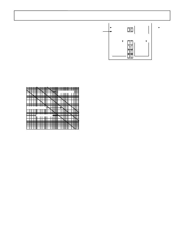
�Figure� 31.� Power� Consumption� Within� the� ADuM640x�
�Both� dynamic� input� and� output� current� is� consumed� only�
�when� operating� at� channel� speeds� higher� than� the� refresh�
�rate,� f� r� .� Each� channel� has� a� dynamic� current� determined� by�
�its� data� rate.� Figure� 23� shows� the� current� for� a� channel� in� the�
�forward� direction,� which� means� that� the� input� is� on� the� primary�
�side� of� the� part.� Figure� 24� shows� the� current� for� a� channel� in� the�
�reverse� direction,� which� means� that� the� input� is� on� the� secondary�
�side� of� the� part.� Both� figures� assume� a� typical� 15� pF� load.� The�
�following� relationship� allows� the� total� I� DD1� current� to� be� calculated:�
�I� DD1� =� (� I� ISO� ×� V� ISO� )/(� E� ×� V� DD1� )� +� ∑� I� CHn� ;� n� =� 1� to� 4�
�(1)�
�10�
�1�
�0.1�
�DISTANCE = 100mm�
�DISTANCE = 5mm�
�where:�
�I� DD1� is� the� total� supply� input� current.�
�I� ISO� is� the� current� drawn� by� the� secondary� side� external� loads.�
�E� is� the� power� supply� efficiency� at� the� maximum� load� from�
�Figure� 13� at� the� V� ISO� and� V� DD1� condition� of� interest.�
�I� CHn� is� the� current� drawn� by� a� single� channel,� determined� from�
�Figure� 23� or� Figure� 24,� depending� on� channel� direction.�
�0.01�
�1k�
�10k�
�100k�
�1M�
�10M�
�100M�
�Calculate� the� maximum� external� load� by� subtracting� the�
�MAGNETIC� FIELD� FREQUENCY� (Hz)�
�dynamic� output� load� from� the� maximum� allowable� load.�
�Figure� 30.� Maximum� Allowable� Current�
�for� Various� Current-to-� ADuM640x� Spacings�
�I� ISO(LOAD)� =� I� ISO(MAX)� ?� ∑� I� ISO(D)n� ;� n� =� 1� to� 4�
�(2)�
�Note� that� at� combinations� of� strong� magnetic� field� and� high�
�frequency,� any� loops� formed� by� PCB� traces� can� induce� error�
�voltages� sufficiently� large� to� trigger� the� thresholds� of� succeeding�
�circuitry.� Exercise� care� in� the� layout� of� such� traces� to� avoid� this�
�possibility.�
�POWER� CONSUMPTION�
�The� V� DD1� power� supply� input� provides� power� to� the� i� Coupler� data�
�channels� as� well� as� to� the� power� converter.� For� this� reason,� the�
�quiescent� currents� drawn� by� the� data� converter� and� the� primary�
�and� secondary� input/output� channels� cannot� be� determined�
�separately.� All� of� these� quiescent� power� demands� are� combined�
�into� the� I� DD1(Q)� current� shown� in� Figure� 31.� The� total� I� DD1� supply�
�current� is� the� sum� of� the� quiescent� operating� current,� the� dynamic�
�current� I� DD1(D)� demanded� by� the� I/O� channels,� and� any� external�
�I� ISO� load.�
�where:�
�I� ISO(LOAD)� is� the� current� available� to� supply� an� external� secondary�
�side� load.�
�I� ISO(MAX)� is� the� maximum� external� secondary� side� load� current�
�available� at� V� ISO� .�
�I� ISO(D)n� is� the� dynamic� load� current� drawn� from� V� ISO� by� an� input�
�or� output� channel,� as� shown� in� Figure� 23� and� Figure� 24� for� a�
�typical� 15� pF� load.�
�This� analysis� assumes� a� 15� pF� capacitive� load� on� each� data� output.�
�If� the� capacitive� load� is� larger� than� 15� pF,� the� additional� current�
�must� be� included� in� the� analysis� of� I� DD1� and� I� ISO(LOAD)� .�
�To� determine� I� DD1� in� Equation� 1,� additional� primary� side�
�dynamic� output� current� (I� AOD� )� is� added� directly� to� I� DD1� .�
�Additional� secondary� side� dynamic� output� current� (I� AOD� )�
�is� added� to� I� ISO� on� a� per-channel� basis.�
�To� determine� I� ISO(LOAD)� in� Equation� 2,� additional� secondary�
�side� output� current� (I� AOD� )� is� subtracted� from� I� ISO(MAX)� on� a�
�per-channel� basis.�
�Rev.� A� |� Page� 23� of� 28�
�相关PDF资料 |
PDF描述 |
|---|---|
| 3610KL-04W-B30-G00 | FAN DC AXIAL 12V 92X25 2450 RPM |
| AWP24-8241-T-R | CONN SOCKET IDC 24POS W/STR GOLD |
| AWP30-8541-T-R | CONN SOCKET IDC 30POS W/STR TIN |
| M80-8411442 | CONN HDR 2MM R/A DUAL 14POS |
| ADUM6404CRWZ | IC ISOLATOR 4CH DCDC CONV 16SOIC |
相关代理商/技术参数 |
参数描述 |
|---|---|
| ADUM6401CRWZ-RL | 功能描述:IC ISOLATOR 4CH DCDC CONV 16SOIC RoHS:是 类别:隔离器 >> 数字隔离器 系列:IsoPower®, iCoupler® 产品培训模块:IsoLoop® Isolator 标准包装:50 系列:IsoLoop® 输入 - 1 侧/2 侧:5/0 通道数:5 电源电压:3 V ~ 5.5 V 电压 - 隔离:2500Vrms 数据速率:110Mbps 传输延迟:12ns 输出类型:CMOS 封装/外壳:16-SOIC(0.154",3.90mm 宽) 供应商设备封装:16-SOIC N 包装:管件 工作温度:-40°C ~ 85°C 其它名称:390-1053-5 |
| ADUM6402 | 制造商:AD 制造商全称:Analog Devices 功能描述:Quad-Channel Isolators with Integrated DC-to-DC Converter |
| ADUM6402ARIZ | 功能描述:隔离器接口集成电路 8mm creepage 4-Ch 5kV Dig Iso Int DC/DC RoHS:否 制造商:Texas Instruments 通道数量:2 传播延迟时间: 电源电压-最大:5.5 V 电源电压-最小:3 V 电源电流:3.6 mA 功率耗散: 最大工作温度:+ 125 C 安装风格: 封装 / 箱体:SOIC-8 封装:Tube |
| ADUM6402ARIZ-RL | 功能描述:隔离器接口集成电路 8mm creepage 4-Ch 5kV Dig Iso Int DC/DC RoHS:否 制造商:Texas Instruments 通道数量:2 传播延迟时间: 电源电压-最大:5.5 V 电源电压-最小:3 V 电源电流:3.6 mA 功率耗散: 最大工作温度:+ 125 C 安装风格: 封装 / 箱体:SOIC-8 封装:Tube |
| ADUM6402ARWZ | 功能描述:IC ISOLATOR 4CH DCDC CONV 16SOIC RoHS:是 类别:隔离器 >> 数字隔离器 系列:IsoPower®, iCoupler® 标准包装:66 系列:iCoupler® 输入 - 1 侧/2 侧:2/2 通道数:4 电源电压:3.3V,5V 电压 - 隔离:2500Vrms 数据速率:25Mbps 传输延迟:60ns 输出类型:逻辑 封装/外壳:20-SSOP(0.209",5.30mm 宽) 供应商设备封装:20-SSOP 包装:管件 工作温度:-40°C ~ 105°C |
发布紧急采购,3分钟左右您将得到回复。