- 您现在的位置:买卖IC网 > PDF目录8963 > ADV7123JSTZ330 (Analog Devices Inc)IC DAC VIDEO 3CH 330MHZ 48-LQFP PDF资料下载
参数资料
| 型号: | ADV7123JSTZ330 |
| 厂商: | Analog Devices Inc |
| 文件页数: | 11/24页 |
| 文件大小: | 0K |
| 描述: | IC DAC VIDEO 3CH 330MHZ 48-LQFP |
| 产品培训模块: | Data Converter Fundamentals DAC Architectures |
| 标准包装: | 1 |
| 位数: | 10 |
| 数据接口: | 并联 |
| 转换器数目: | 3 |
| 电压电源: | 单电源 |
| 功率耗散(最大): | 30mW |
| 工作温度: | 0°C ~ 70°C |
| 安装类型: | 表面贴装 |
| 封装/外壳: | 48-LQFP |
| 供应商设备封装: | 48-LQFP(7x7) |
| 包装: | 托盘 |
| 输出数目和类型: | 6 电流,单极 |
| 采样率(每秒): | 330M |
| 产品目录页面: | 785 (CN2011-ZH PDF) |
ADV7123
Rev. D | Page 19 of 24
Figure 23 shows the video waveforms associated with the three
RGB outputs driving the doubly terminated 75 Ω load of Figure 24.
As well as the gray scale levels, black level to white level, Figure 23
also shows the contributions of SYNC and BLANK for the
ADV7123. These control inputs add appropriately weighted
currents to the analog outputs, producing the specific output
level requirements for video applications.
details how
the
SYNC and BLANK inputs modify the output levels.
GRAY SCALE OPERATION
The ADV7123 can be used for standalone, gray scale (mono-
chrome), or composite video applications (that is, only one
channel used for video information). Any one of the three
channels, red, green, or blue, can be used to input the digital
video data. The two unused video data channels should be tied
to Logic 0. The unused analog outputs should be terminated
with the same load as that for the used channel; that is, if the
red channel is used and IOR is terminated with a doubly
terminated 75 Ω load (37.5 Ω), IOB and IOG should be
terminated with 37.5 Ω resistors (see Figure 26).
R0
R9
G0
ADV7123
G9
B0
B9
IOR
IOG
37.5
DOUBLY
TERMINATED
7.5
LOAD
VIDEO
OUTPUT
37.5
IOB
GND
0
02
15
-0
26
Figure 26. Input and Output Connections for Standalone Gray Scale or
Composite Video
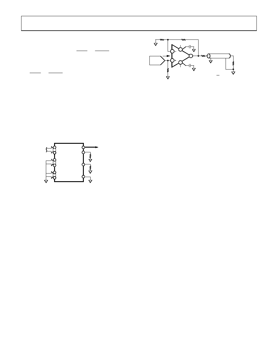
VIDEO OUTPUT BUFFERS
The ADV7123 is specified to drive transmission line loads. The
analog output configuration to drive such loads is described in
the Analog Outputs section and illustrated in Figure 27. However,
in some applications it may be required to drive long transmis-
sion line cable lengths. Cable lengths greater than 10 meters can
attenuate and distort high frequency analog output pulses. The
inclusion of output buffers compensates for some cable distortion.
Buffers with large full power bandwidths and gains between
two and four are required. These buffers also need to be able to
supply sufficient current over the complete output voltage swing.
Analog Devices produces a range of suitable op amps for such
AD848 series of monolithic op amps. In very high frequency
applications (80 MHz), the AD8061 is recommended. More
information on line driver buffering circuits is given in the
relevant op amp data sheets.
Use of buffer amplifiers also allows implementation of other
video standards besides RS-343A and RS-170. Altering the gain
components of the buffer circuit results in any desired video level.
3
6
2
ZL = 75
(MONITOR)
Z0 = 75
Z2
Z1
+VS
–VS
0.1F
75
(CABLE)
GAIN (G) = 1 +
DACs
IOR, IOG, IOB
ZS = 75
(SOURCE
TERMINATION)
AD848
7
4
Z1
Z2
00
21
5-
0
27
Figure 27. AD848 As an Output Buffer
PCB LAYOUT CONSIDERATIONS
The ADV7123 is optimally designed for lowest noise perfor-
mance, both radiated and conducted noise. To complement the
excellent noise performance of the ADV7123, it is imperative
that great care be given to the PCB layout. Figure 28 shows a
recommended connection diagram for the ADV7123.
The layout should be optimized for lowest noise on the
ADV7123 power and ground lines. This can be achieved by
shielding the digital inputs and providing good decoupling.
Shorten the lead length between groups of VAA and GND pins
to minimize inductive ringing.
It is recommended to use a 4-layer printed circuit board with a
single ground plane. The ground and power planes should
separate the signal trace layer and the solder side layer. Noise
on the analog power plane can be further reduced by using
multiple decoupling capacitors (see Figure 28). Optimum
performance is achieved by using 0.1 μF and 0.01 μF ceramic
capacitors. Individually decouple each VAA pin to ground by
placing the capacitors as close as possible to the device with the
capacitor leads as short as possible, thus minimizing lead
inductance. It is important to note that while the ADV7123
contains circuitry to reject power supply noise, this rejection
decreases with frequency. If a high frequency switching power
supply is used, pay close attention to reducing power supply
noise. A dc power supply filter (Murata BNX002) provides EMI
suppression between the switching power supply and the main
PCB. Alternatively, consideration can be given to using a 3-
terminal voltage regulator.
DIGITAL SIGNAL INTERCONNECT
Isolate the digital signal lines to the ADV7123 as much as
possible from the analog outputs and other analog circuitry.
Digital signal lines should not overlay the analog power plane.
Due to the high clock rates used, long clock lines to the
ADV7123 should be avoided to minimize noise pickup.
Connect any active pull-up termination resistors for the digital
inputs to the regular PCB power plane (VCC) and not the analog
power plane.
相关PDF资料 |
PDF描述 |
|---|---|
| MS27484T24B4P | CONN PLUG 56POS STRAIGHT W/PINS |
| VI-263-MW-S | CONVERTER MOD DC/DC 24V 100W |
| VI-263-MW-F4 | CONVERTER MOD DC/DC 24V 100W |
| VI-263-MW-F3 | CONVERTER MOD DC/DC 24V 100W |
| MS27484E16A6S | CONN PLUG 6POS STRAIGHT W/SCKT |
相关代理商/技术参数 |
参数描述 |
|---|---|
| ADV7123KST140 | 制造商:Analog Devices 功能描述:DAC 3-CH Segment 10-bit 48-Pin LQFP 制造商:Rochester Electronics LLC 功能描述:TRIPLE HIGH SPEED VIDEO DAC I.C. - Bulk 制造商:Analog Devices 功能描述:D/A Converter (D-A) IC |
| ADV7123KST140-REEL | 制造商:Analog Devices 功能描述:DAC 3-CH Segment 10-bit 48-Pin LQFP T/R |
| ADV7123KST140-RL | 制造商:AD 制造商全称:Analog Devices 功能描述:CMOS, 330 MHz Triple 10-Bit High Speed Video DAC |
| ADV7123KST50 | 制造商:Analog Devices 功能描述:DAC 3-CH Segment 10-bit 48-Pin LQFP 制造商:Rochester Electronics LLC 功能描述:TRIPLE HIGH SPEED VIDEO DAC I.C. - Bulk 制造商:Analog Devices 功能描述:IC 10-BIT VIDEO DAC |
| ADV7123KSTZ140 | 功能描述:IC DAC VIDEO TRPL HI SPD 48-LQFP RoHS:是 类别:集成电路 (IC) >> 数据采集 - 数模转换器 系列:- 产品培训模块:Lead (SnPb) Finish for COTS Obsolescence Mitigation Program 标准包装:50 系列:- 设置时间:4µs 位数:12 数据接口:串行 转换器数目:2 电压电源:单电源 功率耗散(最大):- 工作温度:-40°C ~ 85°C 安装类型:表面贴装 封装/外壳:8-TSSOP,8-MSOP(0.118",3.00mm 宽) 供应商设备封装:8-uMAX 包装:管件 输出数目和类型:2 电压,单极 采样率(每秒):* 产品目录页面:1398 (CN2011-ZH PDF) |
发布紧急采购,3分钟左右您将得到回复。