- 您现在的位置:买卖IC网 > PDF目录10972 > ADV7183BKSTZ (Analog Devices Inc)IC VIDEO DECODER NTSC 80-LQFP PDF资料下载
参数资料
| 型号: | ADV7183BKSTZ |
| 厂商: | Analog Devices Inc |
| 文件页数: | 19/100页 |
| 文件大小: | 0K |
| 描述: | IC VIDEO DECODER NTSC 80-LQFP |
| 产品培训模块: | Interfacing AV Converters to Blackfin Processors |
| 标准包装: | 1 |
| 类型: | 视频解码器 |
| 应用: | 投影仪,录音机,安全 |
| 电压 - 电源,模拟: | 3.15 V ~ 3.45 V |
| 电压 - 电源,数字: | 1.65 V ~ 2 V |
| 安装类型: | 表面贴装 |
| 封装/外壳: | 80-LQFP |
| 供应商设备封装: | 80-LQFP(14x14) |
| 包装: | 托盘 |
| 产品目录页面: | 788 (CN2011-ZH PDF) |
第1页第2页第3页第4页第5页第6页第7页第8页第9页第10页第11页第12页第13页第14页第15页第16页第17页第18页当前第19页第20页第21页第22页第23页第24页第25页第26页第27页第28页第29页第30页第31页第32页第33页第34页第35页第36页第37页第38页第39页第40页第41页第42页第43页第44页第45页第46页第47页第48页第49页第50页第51页第52页第53页第54页第55页第56页第57页第58页第59页第60页第61页第62页第63页第64页第65页第66页第67页第68页第69页第70页第71页第72页第73页第74页第75页第76页第77页第78页第79页第80页第81页第82页第83页第84页第85页第86页第87页第88页第89页第90页第91页第92页第93页第94页第95页第96页第97页第98页第99页第100页
ADV7183B
Rev. B | Page 25 of 100
DEF_VAL_EN Default Value Enable, Address 0x0C[0]
This bit forces the use of the default values for Y, Cr, and Cb.
Refer to the descriptions for DEF_Y and DEF_C for additional
information. In this mode, the decoder also outputs a stable
27 MHz clock, HS, and VS.
Setting DEF_VAL_EN to 0 (default) outputs a colored screen
determined by user-programmable Y, Cr, and Cb values when
the decoder free-runs. Free-run mode is turned on and off by the
DEF_VAL_AUTO_EN bit.
Setting DEF_VAL_EN to 1 forces a colored screen output
determined by user-programmable Y, Cr, and Cb values. This
overrides picture data even if the decoder is locked.
DEF_VAL_AUTO_EN Default Value Automatic Enable,
Address 0x0C[1]
This bit enables the automatic usage of the default values for
Y, Cr, and Cb when the ADV7183B cannot lock to the
video signal.
Setting DEF_VAL_AUTO_EN to 0 disables free-run mode. If
the decoder is unlocked, it outputs noise.
Setting DEF_VAL_EN to 1 (default) enables free-run mode. A
colored screen set by the user-programmable Y, Cr, and Cb
values is displayed when the decoder loses lock.
CLAMP OPERATION
The input video is ac-coupled into the ADV7183B through a
0.1 μF capacitor. The recommended range of the input video
signal is 0.5 V to 1.6 V (typically 1 V p-p). If the signal exceeds
this range, it cannot be processed correctly in the decoder. Since
the input signal is ac-coupled into the decoder, its dc value
needs to be restored. This process is referred to as clamping the
video. This section explains the general process of clamping on
the ADV7183B and shows the different ways in which a user
can configure its behavior.
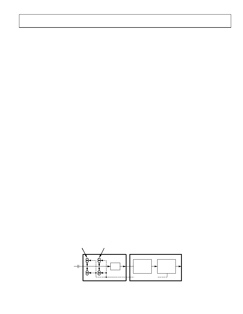
The ADV7183B uses a combination of current sources and a
digital processing block for clamping, as shown in
172H
Figure 10.
The analog processing channel shown is replicated three times
inside the IC. While only one single channel (and only one
ADC) is needed for a CVBS signal, two independent channels
are needed for Y/C (S-VHS) type signals, and three
independent channels are needed to allow component signals
(YPrPb) to be processed.
The clamping can be divided into two sections:
Clamping before the ADC (analog domain): current sources
Clamping after the ADC (digital domain): digital
processing block
The ADCs can digitize an input signal only if it resides within
the ADC’s 1.6 V input voltage range. An input signal with a dc
level that is too large or too small is clipped at the top or bottom
of the ADC range.
The primary task of the analog clamping circuits is to ensure
the video signal stays within the valid ADC input window so
that the analog-to-digital conversion can take place. It is not
necessary to clamp the input signal with a very high accuracy in
the analog domain as long as the video signal fits the ADC range.
After digitization, the digital fine clamp block corrects for any
remaining variations in dc level. Since the dc level of an input
video signal refers directly to the brightness of the picture
transmitted, it is important to perform a fine clamp with high
accuracy; otherwise, brightness variations can occur. Further-
more, dynamic changes in the dc level almost certainly lead to
visually objectionable artifacts and must therefore be prohibited.
The clamping scheme has to be able to acquire a newly connected
video signal with a completely unknown dc level, and it must
maintain the dc level during normal operation.
For quickly acquiring an unknown video signal, the large cur-
rent clamps can be activated. (It is assumed that the amplitude
of the video signal at this point is of a nominal value.) Control
of the coarse and fine current clamp parameters is performed
automatically by the decoder.
Standard definition video signals can have excessive noise on
them. In particular, CVBS signals transmitted by terrestrial
broadcast and demodulated using a tuner usually show very
large levels of noise (>100 mV). A voltage clamp is unsuitable
for this type of video signal. Instead, the ADV7183B uses a set
of four current sources that can cause coarse (>0.5 mA) and fine
(<0.1 mA) currents to flow into and away from the high
impedance node that carries the video signal (see
173H
Figure 10).
COARSE
CURRENT
SOURCES
FINE
CURRENT
SOURCES
DATA
PRE-
PROCESSOR
(DPP)
ADC
SDP
WITH DIGITAL
FINE CLAMP
CLAMP CONTROL
ANALOG
VIDEO
INPUT
04997-010
Figure 10. Clamping Overview
相关PDF资料 |
PDF描述 |
|---|---|
| VI-213-IY-F3 | CONVERTER MOD DC/DC 24V 50W |
| VE-23J-IY-F2 | CONVERTER MOD DC/DC 36V 50W |
| LF10WBR-12P | CONN RCPT WATERPROOF 12POS MALE |
| VI-212-IY-F3 | CONVERTER MOD DC/DC 15V 50W |
| VE-B7N-IX-B1 | CONVERTER MOD DC/DC 18.5V 75W |
相关代理商/技术参数 |
参数描述 |
|---|---|
| ADV7183KST | 制造商:Analog Devices 功能描述:Video Decoder 2ADC 10-Bit 80-Pin LQFP 制造商:Rochester Electronics LLC 功能描述:VIDEO DECODER I.C. - Bulk |
| ADV7184 | 制造商:AD 制造商全称:Analog Devices 功能描述:Multiformat SDTV Video Decoder with Fast Switch Overlay Support |
| ADV7184BSTZ | 功能描述:IC DECODER VID SDTV MULTI 80LQFP RoHS:是 类别:集成电路 (IC) >> 接口 - 编码器,解码器,转换器 系列:- 产品变化通告:Development Systems Discontinuation 26/Apr/2011 标准包装:1 系列:- 类型:编码器 应用:DVB-S.2 系统 电压 - 电源,模拟:- 电压 - 电源,数字:- 安装类型:- 封装/外壳:模块 供应商设备封装:模块 包装:散装 其它名称:Q4645799 |
| ADV7185 | 制造商:AD 制造商全称:Analog Devices 功能描述:Professional NTSC/PAL Video Decoder with 10-Bit CCIR656 Output |
| ADV7185KST | 制造商:AD 制造商全称:Analog Devices 功能描述:Professional NTSC/PAL Video Decoder with 10-Bit CCIR656 Output |
发布紧急采购,3分钟左右您将得到回复。