- 您现在的位置:买卖IC网 > PDF目录15524 > ADZS-BF537-ASKIT (Analog Devices Inc)BOARD EVAL SKIT ADSP-BF537 PDF资料下载
参数资料
| 型号: | ADZS-BF537-ASKIT |
| 厂商: | Analog Devices Inc |
| 文件页数: | 8/68页 |
| 文件大小: | 0K |
| 描述: | BOARD EVAL SKIT ADSP-BF537 |
| 产品培训模块: | Blackfin® Processor Core Architecture Overview Blackfin® Device Drivers Blackfin® Optimizations for Performance and Power Consumption Blackfin® System Services |
| 标准包装: | 1 |
| 系列: | Blackfin® |
| 类型: | DSP:音频 |
| 适用于相关产品: | ADSP-BF537 |
| 所含物品: | 板 |
| 相关产品: | ADSP-BF537KBCZ-6BV-ND - IC DSP CTLR 16BIT 208CSPBGA ADSP-BF537BBCZ-5BV-ND - IC DSP CTLR 16BIT 208CSPBGA ADSP-BF537KBCZ-6AV-ND - IC DSP CTLR 16BIT 182CSPBGA ADSP-BF537BBCZ-5AV-ND - IC DSP CTLR 16BIT 182CSPBGA ADSP-BF537BBCZ-5B-ND - IC DSP CTLR 16BIT 208CSPBGA ADSP-BF537BBC-5A-ND - IC DSP CTLR 16BIT 182CSPBGA |
第1页第2页第3页第4页第5页第6页第7页当前第8页第9页第10页第11页第12页第13页第14页第15页第16页第17页第18页第19页第20页第21页第22页第23页第24页第25页第26页第27页第28页第29页第30页第31页第32页第33页第34页第35页第36页第37页第38页第39页第40页第41页第42页第43页第44页第45页第46页第47页第48页第49页第50页第51页第52页第53页第54页第55页第56页第57页第58页第59页第60页第61页第62页第63页第64页第65页第66页第67页第68页
Rev. J
|
Page 16 of 68
|
February 2014
(VCO) and the system clock. SCLK divider values are 1 through
15. Table 6 illustrates typical system clock ratios.
Note that the divisor ratio must be chosen to limit the system
clock frequency to its maximum of fSCLK. The SSEL value can be
changed dynamically without any PLL lock latencies by writing
the appropriate values to the PLL divisor register (PLL_DIV).
The core clock (CCLK) frequency can also be dynamically
changed by means of the CSEL1–0 bits of the PLL_DIV register.
Supported CCLK divider ratios are 1, 2, 4, and 8, as shown in
Table 7. This programmable core clock capability is useful for
fast core frequency modifications.
The maximum CCLK frequency not only depends on the part’s
speed grade (see Ordering Guide on Page 67), it also depends on
on Page 24 for details). The maximal system clock rate (SCLK)
depends on the chip package and the applied VDDEXT voltage (see
BOOTING MODES
The ADSP-BF534/ADSP-BF536/ADSP-BF537 processor has six
mechanisms (listed in Table 8) for automatically loading inter-
nal and external memory after a reset. A seventh mode is
provided to execute from external memory, bypassing the boot
sequence.
The BMODE pins of the reset configuration register, sampled
during power-on resets and software-initiated resets, imple-
ment the following modes:
Execute from 16-bit external memory – Execution starts
from address 0x2000 0000 with 16-bit packing. The boot
ROM is bypassed in this mode. All configuration settings
are set for the slowest device possible (3-cycle hold time;
15-cycle R/W access times; 4-cycle setup).
Boot from 8-bit and 16-bit external flash memory – The
8-bit or 16-bit flash boot routine located in Boot ROM
memory space is set up using asynchronous memory
bank 0. All configuration settings are set for the slowest
device possible (3-cycle hold time; 15-cycle R/W access
times; 4-cycle setup). The Boot ROM evaluates the first
byte of the boot stream at address 0x2000 0000. If it is 0x40,
8-bit boot is performed. A 0x60 byte assumes a 16-bit
memory device and performs 8-bit DMA. A 0x20 byte also
assumes 16-bit memory but performs 16-bit DMA.
Boot from serial SPI memory (EEPROM or flash) – 8-, 16-,
or 24-bit addressable devices are supported as well as
AT45DB041, AT45DB081, AT45DB161, AT45DB321,
AT45DB642, and AT45DB1282 DataFlash
devices from
Atmel. The SPI uses the PF10/SPI SSEL1 output pin to
select a single SPI EEPROM/flash device, submits a read
command and successive address bytes (0x00) until a valid
8-, 16-, or 24-bit, or Atmel addressable device is detected,
and begins clocking data into the processor.
Boot from SPI host device – The Blackfin processor oper-
ates in SPI slave mode and is configured to receive the bytes
of the .LDR file from an SPI host (master) agent. To hold
off the host device from transmitting while the boot ROM
is busy, the Blackfin processor asserts a GPIO pin, called
host wait (HWAIT), to signal the host device not to send
any more bytes until the flag is deasserted. The flag is cho-
sen by the user and this information is transferred to the
Blackfin processor via bits 10:5 of the FLAG header.
Boot from UART – Using an autobaud handshake
sequence, a boot-stream-formatted program is downloaded
by the host. The host agent selects a baud rate within the
UART’s clocking capabilities. When performing the auto-
baud, the UART expects an “@” (boot stream) character
(8 bits data, 1 start bit, 1 stop bit, no parity bit) on the RXD
pin to determine the bit rate. It then replies with an
acknowledgement that is composed of 4 bytes: 0xBF, the
value of UART_DLL, the value of UART_DLH, and 0x00.
The host can then download the boot stream. When the
processor needs to hold off the host, it deasserts CTS.
Therefore, the host must monitor this signal.
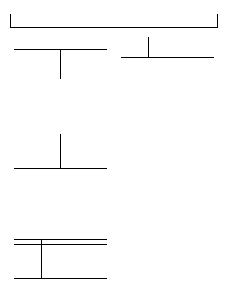
Table 6. Example System Clock Ratios
Signal Name
SSEL3–0
Divider Ratio
VCO:SCLK
Example Frequency Ratios
(MHz)
VCO
SCLK
0001
1:1
100
0110
6:1
300
50
1010
10:1
500
50
Table 7. Core Clock Ratios
Signal Name
CSEL1–0
Divider Ratio
VCO:CCLK
Example Frequency Ratios
(MHz)
VCO
CCLK
00
1:1
300
01
2:1
300
150
10
4:1
500
125
11
8:1
200
25
Table 8. Booting Modes
BMODE2– 0
Description
000
Execute from 16-bit external memory (bypass
boot ROM)
001
Boot from 8-bit or 16-bit memory
(EPROM/flash)
010
Reserved
011
Boot from serial SPI memory (EEPROM/flash)
100
Boot from SPI host (slave mode)
101
Boot from serial TWI memory (EEPROM/flash)
110
Boot from TWI host (slave mode)
111
Boot from UART host (slave mode)
Table 8. Booting Modes (Continued)
BMODE2–0
Description
相关PDF资料 |
PDF描述 |
|---|---|
| ECC18DRAS | CONN EDGECARD 36POS R/A .100 SLD |
| V300C36C75BF | CONVERTER MOD DC/DC 36V 75W |
| SEK100M250ST | CAP ALUM 10UF 250V 20% RADIAL |
| AT91SAM9260-EK | KIT EVAL FOR AT91SAM9260 |
| 1331-271K | INDUCTOR SHIELDED 0.27UH SMD |
相关代理商/技术参数 |
参数描述 |
|---|---|
| ADZS-BF537-EZLITE | 功能描述:BOARD EVAL ADSP-BF537 RoHS:是 类别:编程器,开发系统 >> 通用嵌入式开发板和套件(MCU、DSP、FPGA、CPLD等) 系列:Blackfin® 产品培训模块:Blackfin® Processor Core Architecture Overview Blackfin® Device Drivers Blackfin® Optimizations for Performance and Power Consumption Blackfin® System Services 特色产品:Blackfin? BF50x Series Processors 标准包装:1 系列:Blackfin® 类型:DSP 适用于相关产品:ADSP-BF548 所含物品:板,软件,4x4 键盘,光学拨轮,QVGA 触摸屏 LCD 和 40G 硬盘 配用:ADZS-BFBLUET-EZEXT-ND - EZ-EXTENDER DAUGHTERBOARDADZS-BFLLCD-EZEXT-ND - BOARD EXT LANDSCAP LCD INTERFACE 相关产品:ADSP-BF542BBCZ-4A-ND - IC DSP 16BIT 400MHZ 400CSBGAADSP-BF544MBBCZ-5M-ND - IC DSP 16BIT 533MHZ MDDR 400CBGAADSP-BF542MBBCZ-5M-ND - IC DSP 16BIT 533MHZ MDDR 400CBGAADSP-BF542KBCZ-6A-ND - IC DSP 16BIT 600MHZ 400CSBGAADSP-BF547MBBCZ-5M-ND - IC DSP 16BIT 533MHZ MDDR 400CBGAADSP-BF548BBCZ-5A-ND - IC DSP 16BIT 533MHZ 400CSBGAADSP-BF547BBCZ-5A-ND - IC DSP 16BIT 533MHZ 400CSBGAADSP-BF544BBCZ-5A-ND - IC DSP 16BIT 533MHZ 400CSBGAADSP-BF542BBCZ-5A-ND - IC DSP 16BIT 533MHZ 400CSBGA |
| ADZS-BF537-STAMP | 功能描述:SYSTEM DEV FOR ADSP-BF537 RoHS:是 类别:编程器,开发系统 >> 通用嵌入式开发板和套件(MCU、DSP、FPGA、CPLD等) 系列:Blackfin® 产品培训模块:Blackfin® Processor Core Architecture Overview Blackfin® Device Drivers Blackfin® Optimizations for Performance and Power Consumption Blackfin® System Services 特色产品:Blackfin? BF50x Series Processors 标准包装:1 系列:Blackfin® 类型:DSP 适用于相关产品:ADSP-BF548 所含物品:板,软件,4x4 键盘,光学拨轮,QVGA 触摸屏 LCD 和 40G 硬盘 配用:ADZS-BFBLUET-EZEXT-ND - EZ-EXTENDER DAUGHTERBOARDADZS-BFLLCD-EZEXT-ND - BOARD EXT LANDSCAP LCD INTERFACE 相关产品:ADSP-BF542BBCZ-4A-ND - IC DSP 16BIT 400MHZ 400CSBGAADSP-BF544MBBCZ-5M-ND - IC DSP 16BIT 533MHZ MDDR 400CBGAADSP-BF542MBBCZ-5M-ND - IC DSP 16BIT 533MHZ MDDR 400CBGAADSP-BF542KBCZ-6A-ND - IC DSP 16BIT 600MHZ 400CSBGAADSP-BF547MBBCZ-5M-ND - IC DSP 16BIT 533MHZ MDDR 400CBGAADSP-BF548BBCZ-5A-ND - IC DSP 16BIT 533MHZ 400CSBGAADSP-BF547BBCZ-5A-ND - IC DSP 16BIT 533MHZ 400CSBGAADSP-BF544BBCZ-5A-ND - IC DSP 16BIT 533MHZ 400CSBGAADSP-BF542BBCZ-5A-ND - IC DSP 16BIT 533MHZ 400CSBGA |
| ADZS-BF537-STAMP | 制造商:Analog Devices 功能描述:Microcontroller Development Tool |
| ADZS-BF538-EZLITE | 制造商:Analog Devices 功能描述:- Bulk |
| ADZSBF538FEZLITE | 制造商:Analog Devices 功能描述:RES Wirewound 6927 75Ohm 1% 3W 20PPM SMD T/R |
发布紧急采购,3分钟左右您将得到回复。