- 您现在的位置:买卖IC网 > PDF目录51251 > AF85N08K (INTEGRATED CIRCUIT TECHNOLOGY CORP) 75 A, 80 V, 0.013 ohm, N-CHANNEL, Si, POWER, MOSFET, TO-263AB PDF资料下载
参数资料
| 型号: | AF85N08K |
| 厂商: | INTEGRATED CIRCUIT TECHNOLOGY CORP |
| 元件分类: | JFETs |
| 英文描述: | 75 A, 80 V, 0.013 ohm, N-CHANNEL, Si, POWER, MOSFET, TO-263AB |
| 封装: | ROHS COMPLIANT, TO-263, 3 PIN |
| 文件页数: | 2/6页 |
| 文件大小: | 473K |
| 代理商: | AF85N08K |
AF85N08
N-Channel Enhancement Mode Power MOSFET
Anachip Corp.
www.anachip.com.tw
Rev. 1.0 Aug 10, 2005
2/6
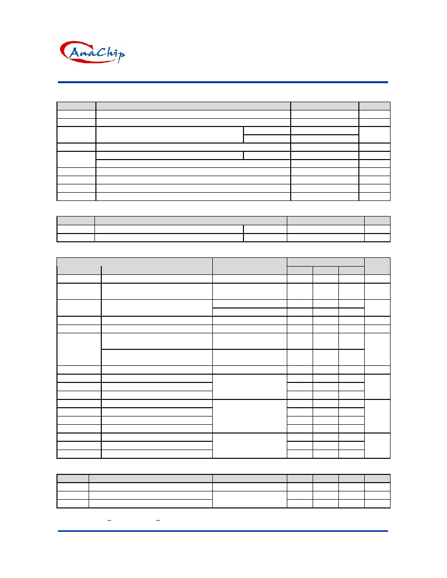
Absolute Maximum Ratings
Symbol
Parameter
Rating
Units
VDS
Drain-Source Voltage
80
V
VGS
Gate-Source Voltage
±20
V
TC=25C
75
ID
Continuous Drain Current, VGS=10V
TC=100C
48
A
IDM
Pulsed Drain Current (Note 1)
260
A
Total Power Dissipation
TC=25C
138
W
PD
Linear Derating Factor
1.11
W/C
EAS
Single Pulse Avalanche Energy (Note 3)
450
mJ
IAR
Avalanche Current
30
A
TSTG
Storage Temperature Range
-55 to 150
C
TJ
Operating Junction Temperature Range
-55 to 150
C
Thermal Data
Symbol
Parameter
Maximum
Units
RθJC
Thermal Resistance Junction-Case
Max.
0.9
C/W
RθJA
Thermal Resistance Junction- Ambient
Max.
62
C/W
Electrical Characteristics (T
J=25C unless otherwise noted)
Limits
Symbol
Parameter
Test Conditions
Min.
Typ.
Max.
Unit
BVDSS
Drain-Source Breakdown Voltage
VGS=0V, ID=1mA
80
-
V
BVDSS/TJ
Breakdown Voltage Temperature
Coefficient
Reference to 25C,
ID=1mA
-
0.09
-
V/C
VGS=10V, ID=45A
-
13
RDS(ON)
Static Drain-Source
On-Resistance (Note 2)
VGS=4.5V, ID=25A
-
18
m
VGS(th)
Gate Threshold Voltage
VDS= VGS, ID=250uA
1
-
3
V
gfs
Forward Transconductance
VDS=10V, ID=45A
-
70
-
S
Drain-Source Leakage
Current(TJ=25C)
VDS=80V, VGS=0V
-
10
IDSS
Drain-Source Leakage
Current(TJ=150C)
VDS=64V, VGS=0V
-
100
uA
IGSS
Gate Source Leakage
VGS=±20V
-
±100
nA
Qg
Total Gate Charge (Note 2)
-
63
100
Qgs
Gate-Source Charge
-
23
-
Qgd
Gate-Drain (“Miller”) Charge
ID=45A
VDS=64V
VGS=4.5V
-
38
-
nC
td(on)
Turn-On Delay Time (Note 2)
-
30
-
tr
Rise Time
-
100
-
td(off)
Turn-Off Delay Time
-
144
-
tf
Fall-Time
VDS=40V
ID=45A
RG=10, VGS=10V
RD=0.89
-
173
-
nS
Ciss
Input Capacitance
-
6300
10080
Coss
Output Capacitance
-
670
-
Crss
Reverse Transfer Capacitance
VGS=0V
VDS=25V,
f=1.0MHz
-
350
-
pF
Source-Drain Diode
Symbol
Parameter
Test Conditions
Min.
Typ.
Max.
Unit
VSD
Forward On Voltage (Note 2)
IS=45A, VGS=0V
-
1.3
V
trr
Reverse Recovery Time (Note 2)
-
47
-
ns
Qrr
Reverse Recovery Charge
IS=20A, VGS=0V,
dl/dt=100A/s
-
86
-
nC
Note 1: Pulse width limited by safe operating area.
Note 2: Pulse width < 300us, duty cycle < 2%.
Note 3: Starting TJ=25
oC, VDD=30V, L=1mH, RG=25, IAS=30A.
相关PDF资料 |
PDF描述 |
|---|---|
| AF85N08KA | 75 A, 80 V, 0.013 ohm, N-CHANNEL, Si, POWER, MOSFET, TO-263AB |
| AF9410NS | 9.6 A, 30 V, 0.018 ohm, N-CHANNEL, Si, POWER, MOSFET |
| AF9410NSL | 9.6 A, 30 V, 0.018 ohm, N-CHANNEL, Si, POWER, MOSFET |
| AF9410NSLA | 9.6 A, 30 V, 0.018 ohm, N-CHANNEL, Si, POWER, MOSFET |
| AF9410NSA | 9.6 A, 30 V, 0.018 ohm, N-CHANNEL, Si, POWER, MOSFET |
相关代理商/技术参数 |
参数描述 |
|---|---|
| AF86-XX | 制造商:ATM 制造商全称:ATM 功能描述:AV/AF86 ATTENUATOR |
| AF87-XX | 制造商:ATM 制造商全称:ATM 功能描述:AV/AF87 ATTENUATOR |
| AF87X-XX | 制造商:ATM 制造商全称:ATM 功能描述:AV/AF87 ATTENUATOR |
| AF88.0 | 制造商:Schneider Electric 功能描述:THERMAL UNIT |
| AF8934 | 功能描述:通用继电器 377 SLD. R RELAY RoHS:否 制造商:Omron Electronics 触点形式:1 Form A (SPST-NO) 触点电流额定值:150 A 线圈电压:24 VDC 线圈电阻:144 Ohms 线圈电流:167 mA 切换电压:400 V 安装风格:Chassis 触点材料: |
发布紧急采购,3分钟左右您将得到回复。