参数资料
| 型号: | AFS1500-2FG484I |
| 厂商: | Microsemi SoC |
| 文件页数: | 289/334页 |
| 文件大小: | 0K |
| 描述: | IC FPGA 8MB FLASH 1.5M 484-FBGA |
| 标准包装: | 60 |
| 系列: | Fusion® |
| RAM 位总计: | 276480 |
| 输入/输出数: | 223 |
| 门数: | 1500000 |
| 电源电压: | 1.425 V ~ 1.575 V |
| 安装类型: | 表面贴装 |
| 工作温度: | -40°C ~ 100°C |
| 封装/外壳: | 484-BGA |
| 供应商设备封装: | 484-FPBGA(23x23) |
第1页第2页第3页第4页第5页第6页第7页第8页第9页第10页第11页第12页第13页第14页第15页第16页第17页第18页第19页第20页第21页第22页第23页第24页第25页第26页第27页第28页第29页第30页第31页第32页第33页第34页第35页第36页第37页第38页第39页第40页第41页第42页第43页第44页第45页第46页第47页第48页第49页第50页第51页第52页第53页第54页第55页第56页第57页第58页第59页第60页第61页第62页第63页第64页第65页第66页第67页第68页第69页第70页第71页第72页第73页第74页第75页第76页第77页第78页第79页第80页第81页第82页第83页第84页第85页第86页第87页第88页第89页第90页第91页第92页第93页第94页第95页第96页第97页第98页第99页第100页第101页第102页第103页第104页第105页第106页第107页第108页第109页第110页第111页第112页第113页第114页第115页第116页第117页第118页第119页第120页第121页第122页第123页第124页第125页第126页第127页第128页第129页第130页第131页第132页第133页第134页第135页第136页第137页第138页第139页第140页第141页第142页第143页第144页第145页第146页第147页第148页第149页第150页第151页第152页第153页第154页第155页第156页第157页第158页第159页第160页第161页第162页第163页第164页第165页第166页第167页第168页第169页第170页第171页第172页第173页第174页第175页第176页第177页第178页第179页第180页第181页第182页第183页第184页第185页第186页第187页第188页第189页第190页第191页第192页第193页第194页第195页第196页第197页第198页第199页第200页第201页第202页第203页第204页第205页第206页第207页第208页第209页第210页第211页第212页第213页第214页第215页第216页第217页第218页第219页第220页第221页第222页第223页第224页第225页第226页第227页第228页第229页第230页第231页第232页第233页第234页第235页第236页第237页第238页第239页第240页第241页第242页第243页第244页第245页第246页第247页第248页第249页第250页第251页第252页第253页第254页第255页第256页第257页第258页第259页第260页第261页第262页第263页第264页第265页第266页第267页第268页第269页第270页第271页第272页第273页第274页第275页第276页第277页第278页第279页第280页第281页第282页第283页第284页第285页第286页第287页第288页当前第289页第290页第291页第292页第293页第294页第295页第296页第297页第298页第299页第300页第301页第302页第303页第304页第305页第306页第307页第308页第309页第310页第311页第312页第313页第314页第315页第316页第317页第318页第319页第320页第321页第322页第323页第324页第325页第326页第327页第328页第329页第330页第331页第332页第333页第334页
Device Architecture
2-42
Revision 4
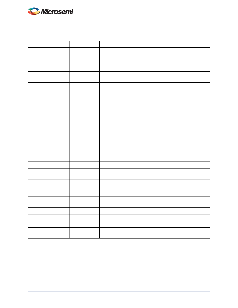
Flash Memory Block Pin Names
Table 2-19 Flash Memory Block Pin Names
Interface Name
Width Direction
Description
ADDR[17:0]
18
In
Byte offset into the FB. Byte-based address.
AUXBLOCK
1
In
When asserted, the page addressed is used to access the auxiliary
block within that page.
BUSY
1
Out
When asserted, indicates that the FB is performing an operation.
CLK
1
In
User interface clock. All operations and status are synchronous to the
rising edge of this clock.
DATAWIDTH[1:0]
2
In
Data width
00 = 1 byte in RD/WD[7:0]
01 = 2 bytes in RD/WD[15:0]
1x = 4 bytes in RD/WD[31:0]
DISCARDPAGE
1
In
When asserted, the contents of the Page Buffer are discarded so that
a new page write can be started.
ERASEPAGE
1
In
When asserted, the address page is to be programmed with all zeros.
ERASEPAGE must transition synchronously with the rising edge of
CLK.
LOCKREQUEST
1
In
When asserted, indicates to the JTAG controller that the FPGA
interface is accessing the FB.
OVERWRITEPAGE
1
In
When asserted, the page addressed is overwritten with the contents of
the Page Buffer if the page is writable.
OVERWRITEPROTECT
1
In
When asserted, all program operations will set the overwrite protect bit
of the page being programmed.
PAGESTATUS
1
In
When asserted with REN, initiates a read page status operation.
PAGELOSSPROTECT
1
In
When asserted, a modified Page Buffer must be programmed or
discarded before accessing a new page.
PIPE
1
In
Adds a pipeline stage to the output for operation above 50 MHz.
PROGRAM
1
In
When asserted, writes the contents of the Page Buffer into the FB
page addressed.
RD[31:0]
32
Out
Read data; data will be valid from the first non-busy cycle (BUSY = 0)
after REN has been asserted.
READNEXT
1
In
When asserted with REN, initiates a read-next operation.
REN
1
In
When asserted, initiates a read operation.
RESET
1
In
When asserted, resets the state of the FB (active low).
SPAREPAGE
1
In
When asserted, the sector addressed is used to access the spare
page within that sector.
相关PDF资料 |
PDF描述 |
|---|---|
| AFS1500-2FGG484I | IC FPGA 8MB FLASH 1.5M 484-FBGA |
| P1AFS1500-2FG484I | IC FPGA PIGEON POINT 484-FBGA |
| ESC40DTEI | CONN EDGECARD 80POS .100 EYELET |
| M1AFS1500-2FGG484I | IC FPGA 8MB FLASH 1.5M 484-FBGA |
| M1AFS1500-2FG484I | IC FPGA 8MB FLASH 1.5M 484-FBGA |
相关代理商/技术参数 |
参数描述 |
|---|---|
| AFS1500-2FG676 | 功能描述:IC FPGA 8MB FLASH 1.5M 676-FBGA RoHS:否 类别:集成电路 (IC) >> 嵌入式 - FPGA(现场可编程门阵列) 系列:Fusion® 产品培训模块:Three Reasons to Use FPGA's in Industrial Designs Cyclone IV FPGA Family Overview 特色产品:Cyclone? IV FPGAs 标准包装:60 系列:CYCLONE® IV GX LAB/CLB数:9360 逻辑元件/单元数:149760 RAM 位总计:6635520 输入/输出数:270 门数:- 电源电压:1.16 V ~ 1.24 V 安装类型:表面贴装 工作温度:0°C ~ 85°C 封装/外壳:484-BGA 供应商设备封装:484-FBGA(23x23) |
| AFS1500-2FG676I | 功能描述:IC FPGA 8MB FLASH 1.5M 676-FBGA RoHS:否 类别:集成电路 (IC) >> 嵌入式 - FPGA(现场可编程门阵列) 系列:Fusion® 标准包装:1 系列:ProASICPLUS LAB/CLB数:- 逻辑元件/单元数:- RAM 位总计:129024 输入/输出数:248 门数:600000 电源电压:2.3 V ~ 2.7 V 安装类型:表面贴装 工作温度:- 封装/外壳:352-BFCQFP,带拉杆 供应商设备封装:352-CQFP(75x75) |
| AFS1500-2FGG256 | 功能描述:IC FPGA 8MB FLASH 1.5M 256-FBGA RoHS:是 类别:集成电路 (IC) >> 嵌入式 - FPGA(现场可编程门阵列) 系列:Fusion® 产品培训模块:Three Reasons to Use FPGA's in Industrial Designs Cyclone IV FPGA Family Overview 特色产品:Cyclone? IV FPGAs 标准包装:60 系列:CYCLONE® IV GX LAB/CLB数:9360 逻辑元件/单元数:149760 RAM 位总计:6635520 输入/输出数:270 门数:- 电源电压:1.16 V ~ 1.24 V 安装类型:表面贴装 工作温度:0°C ~ 85°C 封装/外壳:484-BGA 供应商设备封装:484-FBGA(23x23) |
| AFS1500-2FGG256ES | 制造商:ACTEL 制造商全称:Actel Corporation 功能描述:Actel Fusion Mixed-Signal FPGAs |
| AFS1500-2FGG256I | 功能描述:IC FPGA 8MB FLASH 1.5M 256-FBGA RoHS:是 类别:集成电路 (IC) >> 嵌入式 - FPGA(现场可编程门阵列) 系列:Fusion® 标准包装:1 系列:ProASICPLUS LAB/CLB数:- 逻辑元件/单元数:- RAM 位总计:129024 输入/输出数:248 门数:600000 电源电压:2.3 V ~ 2.7 V 安装类型:表面贴装 工作温度:- 封装/外壳:352-BFCQFP,带拉杆 供应商设备封装:352-CQFP(75x75) |
发布紧急采购,3分钟左右您将得到回复。