参数资料
| 型号: | AFS250-1PQG208I |
| 厂商: | Microsemi SoC |
| 文件页数: | 31/334页 |
| 文件大小: | 0K |
| 描述: | IC FPGA 2MB FLASH 250K 208PQFP |
| 标准包装: | 24 |
| 系列: | Fusion® |
| RAM 位总计: | 36864 |
| 输入/输出数: | 93 |
| 门数: | 250000 |
| 电源电压: | 1.425 V ~ 1.575 V |
| 安装类型: | 表面贴装 |
| 工作温度: | -40°C ~ 100°C |
| 封装/外壳: | 208-BFQFP |
| 供应商设备封装: | 208-PQFP(28x28) |
第1页第2页第3页第4页第5页第6页第7页第8页第9页第10页第11页第12页第13页第14页第15页第16页第17页第18页第19页第20页第21页第22页第23页第24页第25页第26页第27页第28页第29页第30页当前第31页第32页第33页第34页第35页第36页第37页第38页第39页第40页第41页第42页第43页第44页第45页第46页第47页第48页第49页第50页第51页第52页第53页第54页第55页第56页第57页第58页第59页第60页第61页第62页第63页第64页第65页第66页第67页第68页第69页第70页第71页第72页第73页第74页第75页第76页第77页第78页第79页第80页第81页第82页第83页第84页第85页第86页第87页第88页第89页第90页第91页第92页第93页第94页第95页第96页第97页第98页第99页第100页第101页第102页第103页第104页第105页第106页第107页第108页第109页第110页第111页第112页第113页第114页第115页第116页第117页第118页第119页第120页第121页第122页第123页第124页第125页第126页第127页第128页第129页第130页第131页第132页第133页第134页第135页第136页第137页第138页第139页第140页第141页第142页第143页第144页第145页第146页第147页第148页第149页第150页第151页第152页第153页第154页第155页第156页第157页第158页第159页第160页第161页第162页第163页第164页第165页第166页第167页第168页第169页第170页第171页第172页第173页第174页第175页第176页第177页第178页第179页第180页第181页第182页第183页第184页第185页第186页第187页第188页第189页第190页第191页第192页第193页第194页第195页第196页第197页第198页第199页第200页第201页第202页第203页第204页第205页第206页第207页第208页第209页第210页第211页第212页第213页第214页第215页第216页第217页第218页第219页第220页第221页第222页第223页第224页第225页第226页第227页第228页第229页第230页第231页第232页第233页第234页第235页第236页第237页第238页第239页第240页第241页第242页第243页第244页第245页第246页第247页第248页第249页第250页第251页第252页第253页第254页第255页第256页第257页第258页第259页第260页第261页第262页第263页第264页第265页第266页第267页第268页第269页第270页第271页第272页第273页第274页第275页第276页第277页第278页第279页第280页第281页第282页第283页第284页第285页第286页第287页第288页第289页第290页第291页第292页第293页第294页第295页第296页第297页第298页第299页第300页第301页第302页第303页第304页第305页第306页第307页第308页第309页第310页第311页第312页第313页第314页第315页第316页第317页第318页第319页第320页第321页第322页第323页第324页第325页第326页第327页第328页第329页第330页第331页第332页第333页第334页
Device Architecture
2-110
Revision 4
connected between the VAREF and ADCGNDREF pins. The VAREFSEL control pin is used to select the
reference voltage.
ADC Clock
The speed of the ADC depends on its internal clock, ADCCLK, which is not accessible to users. The
ADCCLK is derived from SYSCLK. Input signal TVC[7:0], Time Divider Control, determines the speed of
the ADCCLK in relationship to SYSCLK, based on EQ 15.
EQ 15
TVC: Time Divider Control (0–255)
tADCCLK is the period of ADCCLK, and must be between 0.5 MHz and 10 MHz
tSYSCLK is the period of SYSCLK
The frequency of ADCCLK, fADCCLK, must be within 0.5 Hz to 10 MHz.
The inputs to the ADC are synchronized to SYSCLK. A conversion is initiated by asserting the
ADCSTART signal on a rising edge of SYSCLK. Figure 2-90 on page 2-114 and Figure 2-91 on
page 2-115 show the timing diagram for the ADC.
Acquisition Time or Sample Time Control
Acquisition time (tSAMPLE) specifies how long an analog input signal has to charge the internal capacitor
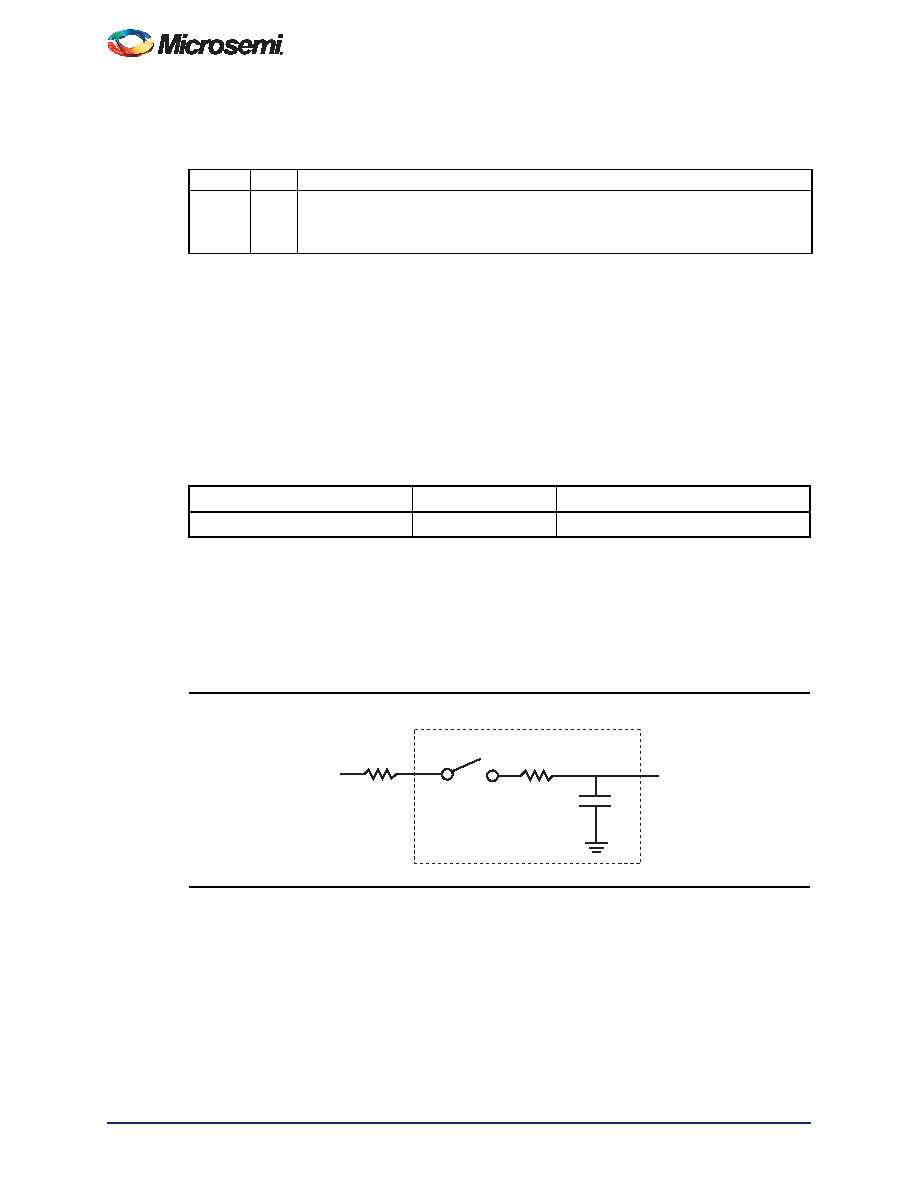
array. Figure 2-88 shows a simplified internal input sampling mechanism of a SAR ADC.
The internal impedance (ZINAD), external source resistance (RSOURCE), and sample capacitor (CINAD)
form a simple RC network. As a result, the accuracy of the ADC can be affected if the ADC is given
insufficient time to charge the capacitor. To resolve this problem, you can either reduce the source
resistance or increase the sampling time by changing the acquisition time using the STC signal.
EQ 16 through EQ 18 can be used to calculate the acquisition time required for a given input. The STC
signal gives the number of sample periods in ADCCLK for the acquisition time of the desired signal. If the
actual acquisition time is higher than the STC value, the settling time error can affect the accuracy of the
ADC, because the sampling capacitor is only partially charged within the given sampling cycle. Example
acquisition times are given in Table 2-44 and Table 2-45. When controlling the sample time for the ADC
Table 2-42 VAREF Bit Function
Name
Bit
Function
VAREF
0
Reference voltage selection
0 – Internal voltage reference selected. VAREF pin outputs 2.56 V.
1 – Input external voltage reference from VAREF and ADCGNDREF
Table 2-43 TVC Bits Function
Name
Bits
Function
TVC
[7:0]
SYSCLK divider control
Figure 2-88 Simplified Sample and Hold Circuitry
tADCCLK
41 TVC
+
tSYSCLK
=
Sample and Hold
ZINAD
CINAD
Rsource
相关PDF资料 |
PDF描述 |
|---|---|
| M1AFS250-1PQ208I | IC FPGA 2MB FLASH 250K 208-PQFP |
| A14V15A-PL84C | IC FPGA 1500 GATES 3.3V 84-PLCC |
| A14V15A-PLG84C | IC FPGA 1500 GATES 3.3V 84-PLCC |
| 5745172-3 | CONN BACKSHELL DB15 DIE CAST |
| AFS250-1PQ208I | IC FPGA 2MB FLASH 250K 208PQFP |
相关代理商/技术参数 |
参数描述 |
|---|---|
| AFS250-1PQG256ES | 制造商:ACTEL 制造商全称:Actel Corporation 功能描述:Actel Fusion Mixed-Signal FPGAs |
| AFS250-1PQG256I | 制造商:ACTEL 制造商全称:Actel Corporation 功能描述:Actel Fusion Mixed-Signal FPGAs |
| AFS250-1PQG256PP | 制造商:ACTEL 制造商全称:Actel Corporation 功能描述:Actel Fusion Mixed-Signal FPGAs |
| AFS250-1QN256ES | 制造商:ACTEL 制造商全称:Actel Corporation 功能描述:Actel Fusion Mixed-Signal FPGAs |
| AFS250-1QN256I | 制造商:ACTEL 制造商全称:Actel Corporation 功能描述:Actel Fusion Mixed-Signal FPGAs |
发布紧急采购,3分钟左右您将得到回复。