- 您现在的位置:买卖IC网 > PDF目录294985 > AGLP060V5CS289I FPGA, 1584 CLBS, 60000 GATES, PBGA289 PDF资料下载
参数资料
| 型号: | AGLP060V5CS289I |
| 元件分类: | FPGA |
| 英文描述: | FPGA, 1584 CLBS, 60000 GATES, PBGA289 |
| 封装: | 14 X 14 MM , 1.2 MM HEIGHT, 0.8 MM PITCH, CSP-289 |
| 文件页数: | 99/128页 |
| 文件大小: | 4383K |
| 代理商: | AGLP060V5CS289I |
第1页第2页第3页第4页第5页第6页第7页第8页第9页第10页第11页第12页第13页第14页第15页第16页第17页第18页第19页第20页第21页第22页第23页第24页第25页第26页第27页第28页第29页第30页第31页第32页第33页第34页第35页第36页第37页第38页第39页第40页第41页第42页第43页第44页第45页第46页第47页第48页第49页第50页第51页第52页第53页第54页第55页第56页第57页第58页第59页第60页第61页第62页第63页第64页第65页第66页第67页第68页第69页第70页第71页第72页第73页第74页第75页第76页第77页第78页第79页第80页第81页第82页第83页第84页第85页第86页第87页第88页第89页第90页第91页第92页第93页第94页第95页第96页第97页第98页当前第99页第100页第101页第102页第103页第104页第105页第106页第107页第108页第109页第110页第111页第112页第113页第114页第115页第116页第117页第118页第119页第120页第121页第122页第123页第124页第125页第126页第127页第128页
IGLOO PLUS DC and Switching Characteristics
2- 58
R e v i sio n 1 1
Global Tree Timing Characteristics
Global clock delays include the central rib delay, the spine delay, and the row delay. Delays do not
include I/O input buffer clock delays, as these are I/O standard–dependent, and the clock may be driven
and conditioned internally by the CCC module. For more details on clock conditioning capabilities, refer
to the "Clock Conditioning Circuits" section on page 2-61. Table 2-84 to Table 2-89 on page 2-60 present
minimum and maximum global clock delays within each device. Minimum and maximum delays are
measured with minimum and maximum loading.
Timing Characteristics
1.5 V DC Core Voltage
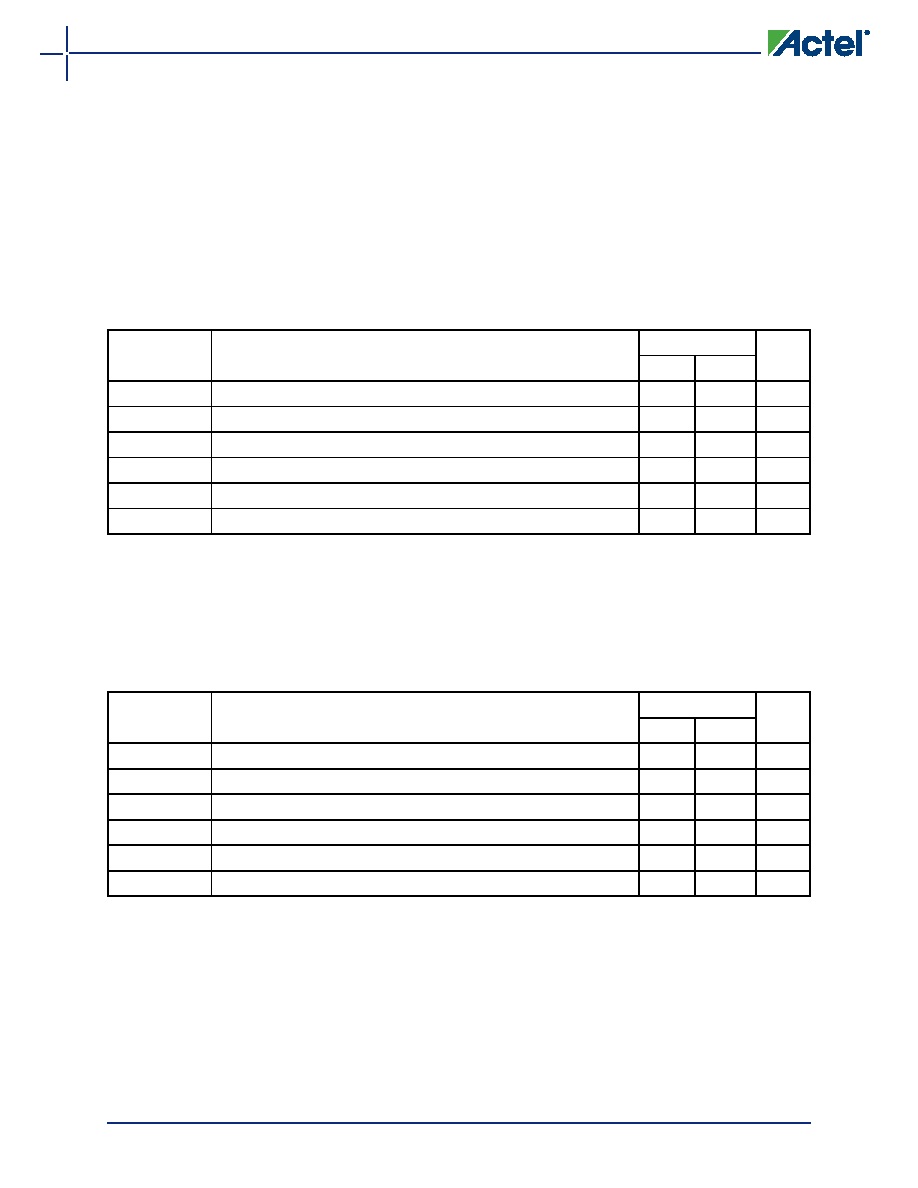
Table 2-84 AGLP030 Global Resource
Commercial-Case Conditions: TJ = 70°C, VCC = 1.425 V
Parameter
Description
Std.
Units
Min.1
Max.2
tRCKL
Input Low Delay for Global Clock
1.21
1.42
ns
tRCKH
Input High Delay for Global Clock
1.23
1.49
ns
tRCKMPWH
Minimum Pulse Width High for Global Clock
ns
tRCKMPWL
Minimum Pulse Width Low for Global Clock
ns
tRCKSW
Maximum Skew for Global Clock
0.27
ns
FRMAX
Maximum Frequency for Global Clock
MHz
Notes:
1. Value reflects minimum load. The delay is measured from the CCC output to the clock pin of a sequential element,
located in a lightly loaded row (single element is connected to the global net).
2. Value reflects maximum load. The delay is measured on the clock pin of the farthest sequential element, located in a fully
loaded row (all available flip-flops are connected to the global net in the row).
3. For specific junction temperature and voltage supply levels, refer to Table 2-6 on page 2-6 for derating values.
Table 2-85 AGLP060 Global Resource
Commercial-Case Conditions: TJ = 70°C, VCC = 1.425 V
Parameter
Description
Std.
Units
Min.1
Max.2
tRCKL
Input Low Delay for Global Clock
1.32
1.62
ns
tRCKH
Input High Delay for Global Clock
1.34
1.72
ns
tRCKMPWH
Minimum Pulse Width High for Global Clock
ns
tRCKMPWL
Minimum Pulse Width Low for Global Clock
ns
tRCKSW
Maximum Skew for Global Clock
0.38
ns
FRMAX
Maximum Frequency for Global Clock
MHz
Notes:
1. Value reflects minimum load. The delay is measured from the CCC output to the clock pin of a sequential element,
located in a lightly loaded row (single element is connected to the global net).
2. Value reflects maximum load. The delay is measured on the clock pin of the farthest sequential element, located in a fully
loaded row (all available flip-flops are connected to the global net in the row).
3. For specific junction temperature and voltage supply levels, refer to Table 2-6 on page 2-6 for derating values.
相关PDF资料 |
PDF描述 |
|---|---|
| AGLP060V5CS289 | FPGA, 1584 CLBS, 60000 GATES, PBGA289 |
| AGLP060V5CSG201I | FPGA, 1584 CLBS, 60000 GATES, PBGA201 |
| AGLP060V5CSG201 | FPGA, 1584 CLBS, 60000 GATES, PBGA201 |
| AGLP060V5CSG289I | FPGA, 1584 CLBS, 60000 GATES, PBGA289 |
| AGLP060V5CSG289 | FPGA, 1584 CLBS, 60000 GATES, PBGA289 |
相关代理商/技术参数 |
参数描述 |
|---|---|
| AGLP060-V5CS289I | 制造商:ACTEL 制造商全称:Actel Corporation 功能描述:IGLOO PLUS Low-Power Flash FPGAs with FlashFreeze Technology |
| AGLP060V5-CS289I | 功能描述:IC FPGA IGLOO PLUS 60K 289-CSP RoHS:否 类别:集成电路 (IC) >> 嵌入式 - FPGA(现场可编程门阵列) 系列:IGLOO PLUS 标准包装:90 系列:ProASIC3 LAB/CLB数:- 逻辑元件/单元数:- RAM 位总计:36864 输入/输出数:157 门数:250000 电源电压:1.425 V ~ 1.575 V 安装类型:表面贴装 工作温度:-40°C ~ 125°C 封装/外壳:256-LBGA 供应商设备封装:256-FPBGA(17x17) |
| AGLP060-V5CS289PP | 制造商:ACTEL 制造商全称:Actel Corporation 功能描述:IGLOO PLUS Low-Power Flash FPGAs with FlashFreeze Technology |
| AGLP060V5-CSG201 | 功能描述:IC FPGA IGLOO PLUS 60K 201-CSP RoHS:是 类别:集成电路 (IC) >> 嵌入式 - FPGA(现场可编程门阵列) 系列:IGLOO PLUS 标准包装:152 系列:IGLOO PLUS LAB/CLB数:- 逻辑元件/单元数:792 RAM 位总计:- 输入/输出数:120 门数:30000 电源电压:1.14 V ~ 1.575 V 安装类型:表面贴装 工作温度:-40°C ~ 85°C 封装/外壳:289-TFBGA,CSBGA 供应商设备封装:289-CSP(14x14) |
| AGLP060V5-CSG201I | 功能描述:IC FPGA IGLOO PLUS 60K 201-CSP RoHS:是 类别:集成电路 (IC) >> 嵌入式 - FPGA(现场可编程门阵列) 系列:IGLOO PLUS 标准包装:152 系列:IGLOO PLUS LAB/CLB数:- 逻辑元件/单元数:792 RAM 位总计:- 输入/输出数:120 门数:30000 电源电压:1.14 V ~ 1.575 V 安装类型:表面贴装 工作温度:-40°C ~ 85°C 封装/外壳:289-TFBGA,CSBGA 供应商设备封装:289-CSP(14x14) |
发布紧急采购,3分钟左右您将得到回复。