- 您现在的位置:买卖IC网 > PDF目录92913 > AH11-G (TRIQUINT SEMICONDUCTOR INC) 150 MHz - 3000 MHz RF/MICROWAVE WIDE BAND MEDIUM POWER AMPLIFIER PDF资料下载
参数资料
| 型号: | AH11-G |
| 厂商: | TRIQUINT SEMICONDUCTOR INC |
| 元件分类: | 放大器 |
| 英文描述: | 150 MHz - 3000 MHz RF/MICROWAVE WIDE BAND MEDIUM POWER AMPLIFIER |
| 封装: | GREEN, MS-012, SMT, SOIC-8 |
| 文件页数: | 5/6页 |
| 文件大小: | 322K |
| 代理商: | AH11-G |
Specifications and information are subject to change without notice
TriQuint Semiconductor, Inc
Phone 1-800-WJ1-4401 FAX: 408-577-6633 e-mail: info-sales@tqs.com Web site: www. TriQuint.com
Page 5 of 6 December 2008
AH11
High Dynamic Range Dual Amplifier
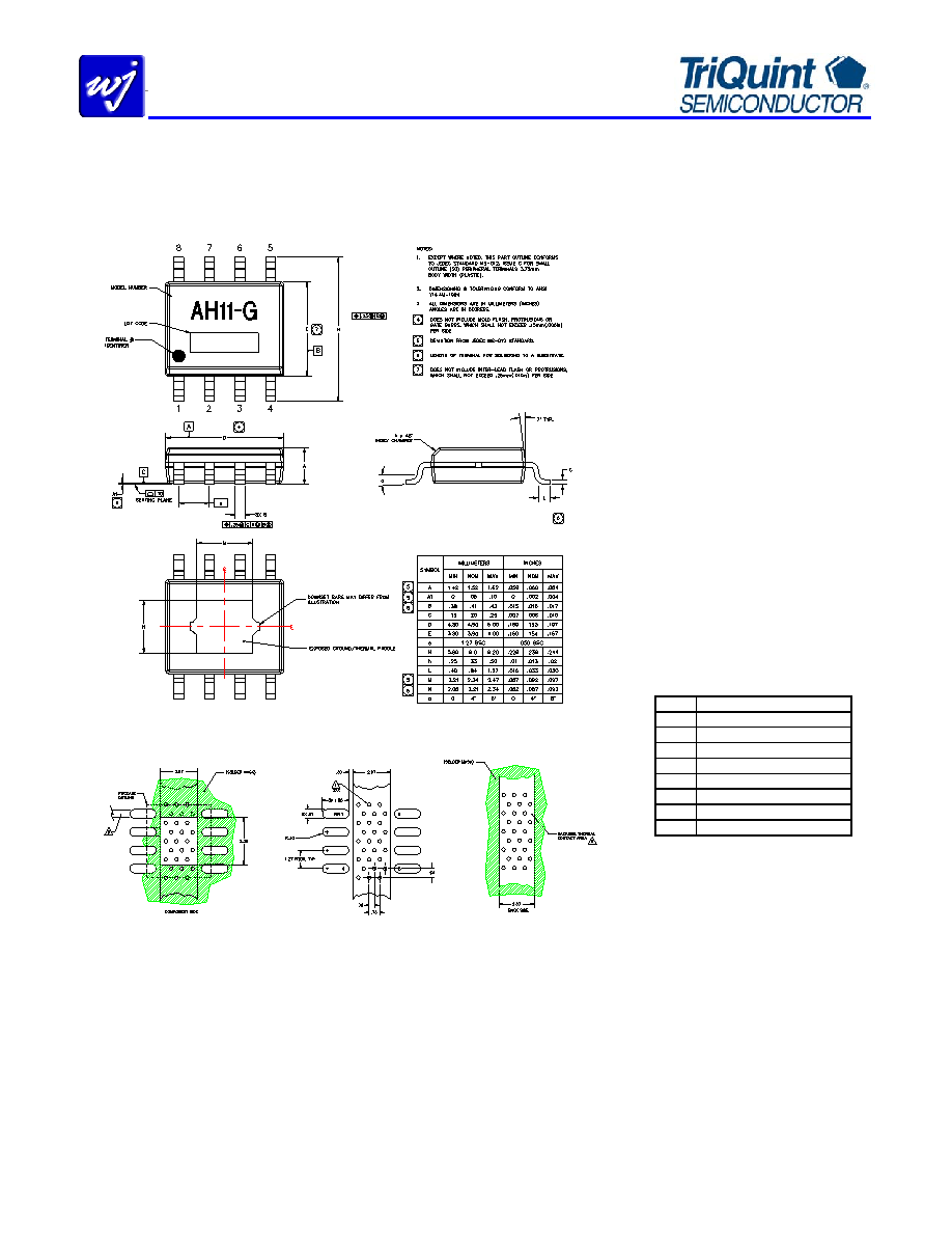
AH11-G Mechanical Information
This package is lead-free/Green/RoHS-compliant. The plating material on the leads is NiPdAu. It is compatible with both
lead-free (maximum 260
°C reflow temperature) and lead (maximum 245 °C reflow temperature) soldering processes.
Outline Drawing
Land Pattern
Product Marking
The component will be marked with an
“AH11-G” designator with an alphanumeric
lot code on the top surface of the package.
The obsolete tin-lead package is marked with
an
“AH11”
designator
followed
by
an
alphanumeric lot code.
Tape and reel specifications for this part are
located on the website in the “Application
Notes” section.
ESD / MSL Information
ESD Rating:
Class 1B
Value:
Passes from 500 to 1000 V
Test:
Human Body Model (HBM)
Standard:
JEDEC Standard JESD22-A114
ESD Rating:
Class IV
Value
Passes greater than 1000 V
Test:
Charge Device Model (CDM)
Standard:
JEDEC Standard JESD22-C101
MSL Rating: Level 2 at +260
°C convection reflow
Standard:
JEDEC Standard J-STD-020A
Functional Pin Layout
Pin
Function
1
RF input (Amp1 input)
2
Ground
3
Ground
4
RF input (Amp2 input)
5
RF output (Amp2 output)
6
Ground
7
Ground
8
RF output (Amp1 output)
The backside paddle is the Source and should be
grounded for thermal and electrical purposes.
Mounting Config. Notes
1.
Ground / thermal vias are critical for the proper performance
of this device.
Vias should use a .35mm (#80/.0135”)
diameter drill and have a final plated through diameter
of .25mm (.010”)
2.
Add as much copper as possible to inner and outer layers
near the part to ensure optimal thermal performance.
3.
To ensure reliable operation, device ground paddle-to-
ground pad solder joint is critical.
4.
Add mounting screws near the part to fasten the board to a
heatsink.
Ensure that the ground / thermal via region
contacts the heatsink.
5.
For optimal thermal performance, expose soldermask on
backside where it contacts the heatsink.
6.
RF trace width depends upon the PC board material and
construction.
7.
Use 1 oz. Copper minimum.
8.
If the PCB design rules allow, ground vias should be placed
under the land pattern for better RF and thermal performance.
Otherwise ground vias should be placed as close to the land
pattern as possible.
9.
All dimensions are in mm. Angles are in degrees.
相关PDF资料 |
PDF描述 |
|---|---|
| AH110-89 | 50 MHz - 2000 MHz RF/MICROWAVE WIDE BAND MEDIUM POWER AMPLIFIER |
| AH110-89 | 50 MHz - 2000 MHz RF/MICROWAVE WIDE BAND MEDIUM POWER AMPLIFIER |
| AH115-S8G | 1800 MHz - 2300 MHz RF/MICROWAVE NARROW BAND MEDIUM POWER AMPLIFIER |
| AH115-S8 | 1800 MHz - 2300 MHz RF/MICROWAVE NARROW BAND MEDIUM POWER AMPLIFIER |
| AH115-S8 | 1800 MHz - 2300 MHz RF/MICROWAVE NARROW BAND MEDIUM POWER AMPLIFIER |
相关代理商/技术参数 |
参数描述 |
|---|---|
| AH11PP1900-PCB | 功能描述:射频开发工具 1900MHz Push-Pull Eval Brd 12dB Gain RoHS:否 制造商:Taiyo Yuden 产品:Wireless Modules 类型:Wireless Audio 工具用于评估:WYSAAVDX7 频率: 工作电源电压:3.4 V to 5.5 V |
| AH11PP900-PCB | 功能描述:射频开发工具 900MHz Push-Pull Eval Brd 13dB Gain RoHS:否 制造商:Taiyo Yuden 产品:Wireless Modules 类型:Wireless Audio 工具用于评估:WYSAAVDX7 频率: 工作电源电压:3.4 V to 5.5 V |
| AH11TRG | 制造商:TriQuint Semiconductor 功能描述:GAIN BLOCK |
| AH1201GY | 制造商:Cooper Wiring Devices 功能描述: |
| AH1201LTVM | 制造商:Cooper Wiring Devices 功能描述: |
发布紧急采购,3分钟左右您将得到回复。