- 您现在的位置:买卖IC网 > PDF目录166131 > AK4101A (Asahi Kasei Microsystems Co.,Ltd) QUAD OUTPUTS 192KHZ 24 BIT DIT PDF资料下载
参数资料
| 型号: | AK4101A |
| 厂商: | Asahi Kasei Microsystems Co.,Ltd |
| 英文描述: | QUAD OUTPUTS 192KHZ 24 BIT DIT |
| 中文描述: | 四输出192kHz的24位动态网 |
| 文件页数: | 24/29页 |
| 文件大小: | 317K |
| 代理商: | AK4101A |
第1页第2页第3页第4页第5页第6页第7页第8页第9页第10页第11页第12页第13页第14页第15页第16页第17页第18页第19页第20页第21页第22页第23页当前第24页第25页第26页第27页第28页第29页
ASAHI KASEI
[AK4101A]
MS0250-E-00
2003/07
- 4 -
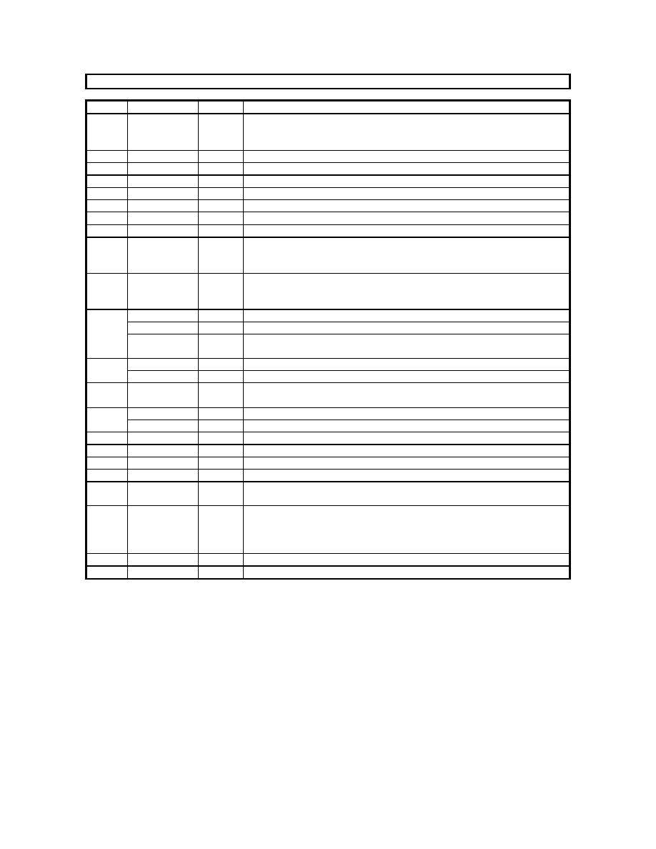
PIN/FUNCTION
No.
Pin Name
I/O
Function
1
PDN
I
Power Down & Reset Pin
(Pull-up Pin)
When “L”, the AK4101A is powered-down, TXP/N pins are “L” and the
control registers are reset to default values.
2
MCLK
I
Master Clock Input Pin
3
SDTI1
I
Audio Serial Data Input 1 Pin
4
SDTI2
I
Audio Serial Data Input 2 Pin
(Pull-down Pin)
5
SDTI3
I
Audio Serial Data Input 3 Pin
(Pull-down Pin)
6
SDTI4
I
Audio Serial Data Input 4 Pin
(Pull-down Pin)
7
VDD
-
Power Supply Pin, 4.75V
5.25V
8
VSS
-
Ground Pin, 0V
9
BICK
I/O
Audio Serial Data Clock Input/Output Pin
Serial Clock for SDTI pins which can be configured as an output based on
the DIF2-0 inputs.
10
LRCK
I/O
Input/Output Channel Clock Pin
Indicates left or right channel, and can be configured as an output based on
the DIF2-0 inputs.
FS0
I
Sampling Frequency Select 0 Pin at Synchronous mode (Pull-down Pin)
CSN
I
Host Interface Chip Select Pin at Asynchronous mode (Pull-down Pin)
11
AKMODE
I
AK4112B Mode Pin at Audio routing mode
(Pull-down Pin)
0: Non-AKM receivers mode, 1: AK4112B mode
FS1
I
Sampling Frequency Select 1 Pin at Synchronous mode (Pull-down Pin)
12
CDTI
I
Host Interface Data Input Pin at Asynchronous mode
(Pull-down Pin)
FS2
I
Sampling Frequency Select 2 Pin at Synchronous mode (Pull-down Pin)
13
CCLK
I
Host Interface Bit Clock Input Pin at Asynchronous mode (Pull-down Pin)
FS3
I
Sampling Frequency Select 3 Pin at Synchronous mode (Pull-down Pin)
14
CDTO
O
Host Interface Data Output Pin at Asynchronous mode (Pull-down Pin)
15
C1
I
Channel Status Bit Input Pin for Channel 1
16
C2
I
Channel Status Bit Input Pin for Channel 2
(Pull-down Pin)
17
C3
I
Channel Status Bit Input Pin for Channel 3
(Pull-down Pin)
18
C4
I
Channel Status Bit Input Pin for Channel 4
(Pull-down Pin)
19
ANS
I
Asynchronous/Synchronous Mode Select Pin
(Pull-up Pin)
0: Asynchronous mode, 1: Synchronous mode
20
BLS
I/O
Block Start Input/Output Pin
(Pull-down Pin)
In normal mode, the channel status block output is “H” for the first four
bytes. In audio routing mode, the pin is configured as an input. When PDN
pin = “L”, BLS pin goes “H” at Normal mode.
21
CKS0
I
Clock Mode Select 0 Pin
(Pull-up Pin)
22
VSS
-
Ground Pin, 0V
相关PDF资料 |
PDF描述 |
|---|---|
| AK4104ET | SPECIALTY CONSUMER CIRCUIT, PDSO16 |
| AK41128HRM-15LP | 128K X 1 MULTI DEVICE DRAM MODULE, 150 ns, CDIP18 |
| AK41256SR-15LP | 256K X 1 MULTI DEVICE DRAM MODULE, 150 ns, SMA22 |
| AK4112B | HIGH FEATURE 96kHz 24BIT DIR |
| AK4181AVT | TOUCH SCREEN CONTROLLER |
相关代理商/技术参数 |
参数描述 |
|---|---|
| AK4101AVQ | 制造商:AKM 制造商全称:AKM 功能描述:QUAD OUTPUTS 192KHZ 24 BIT DIT |
| AK4101AVQP | 功能描述:IC TX RS422 QUAD 44LQFP RoHS:是 类别:集成电路 (IC) >> 线性 - 音频处理 系列:- 其它有关文件:STA321 View All Specifications 标准包装:1 系列:Sound Terminal™ 类型:音频处理器 应用:数字音频 安装类型:表面贴装 封装/外壳:64-LQFP 裸露焊盘 供应商设备封装:64-LQFP EP(10x10) 包装:Digi-Reel® 其它名称:497-11050-6 |
| AK4101VQ | 制造商:未知厂家 制造商全称:未知厂家 功能描述:Consumer IC |
| AK4102 | 制造商:PULSE 制造商全称:Pulse A Technitrol Company 功能描述:TELECOMMUNICATIONS PRODUCTS |
| AK410-2 | 功能描述:CABLE EXTEN CENT INTERFACE RoHS:否 类别:电缆组件 >> D形,Centronics 系列:- 标准包装:1 系列:- 配置:VHDCI 68 位置公型至公型 长度:10.00'(3.05m) 缆线类型:圆形 - 黑色 屏蔽:屏蔽 样式:SCSI Ultra 2 |
发布紧急采购,3分钟左右您将得到回复。