- 您现在的位置:买卖IC网 > PDF目录166131 > AK4532-E2 SPECIALTY CONSUMER CIRCUIT, PDSO24 PDF资料下载
参数资料
| 型号: | AK4532-E2 |
| 元件分类: | 消费家电 |
| 英文描述: | SPECIALTY CONSUMER CIRCUIT, PDSO24 |
| 封装: | 0.65 MM PITCH, PLASTIC, VSOP-24 |
| 文件页数: | 15/17页 |
| 文件大小: | 239K |
| 代理商: | AK4532-E2 |
ASAHI KASEI
[AK4532]
0178-E-02
7
2004/12
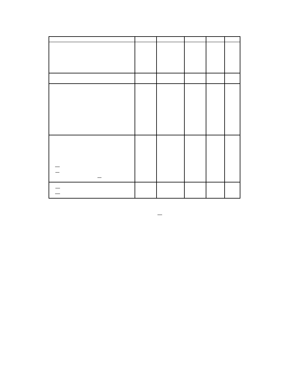
SWITCHING CHARACTERISTICS
(Ta=25
°C; VA, VD = 5.0V ± 10%, CL = 20pF)
Parameter
Symbol
min
typ
max
Units
Master Clock Timing (CMODE=L)
(CMODE=H)
Pulse Width Low
(CMODE=L)
(CMODE=H)
Pulse Width High
(CMODE=L)
(CMODE=H)
fCLK
fCLKL
fCLKH
1.024
1.536
31.25
23
31.25
23
11.2896
16.9344
12.800
19.2
MHz
ns
LRCK Frequency (Note 1)
Duty Cycle
fs
4
45
44.1
50
55
kHz
%
Serial Interface Timing
SCLK Period
SCLK Pulse Width Low
SCLK Pulse Width High
LRCK Edge to SCLK “rising edge” (Note 2)
SCLK “rising edge” to LRCK edge (Note 2)
SDI Hold Time
SDI Setup Time
LRCK to SDO(MSB)
SCLK “rising edge” to SDO
tSCK
tSCKL
tSCKH
tLRS
tSLR
tSDH
tSDS
tLRS
tSSD
312.5
100
50
70
ns
Control Interface Timing
CCLK Period
CCLK Pulse Width Low
CCLK Pulse Width High
CDATA Hold Time
CDATA Setup Time
CS High Level Time
CS “falling edge” to CCLK “rising” time
CCLK “rising time” to CS “rising” time
tCCK
tCCKL
tCCKH
tCDS
tCDH
tCSW
tCSS
tCSH
200 (Note 4)
80
50
150 (Note 4)
50 (Note 4)
50
ns
Reset Timing
PD Pulse Width
PD “rising edge” to SDO delay (Note 3)
tPD
tPDS
150
516
ns
1/fs
Note: 1. If the duty of LRCK changes larger than 5% from 50%, the AK4532 is reset by the internal
phase detecting circuit automatically.
2. SCLK rising edge must not occur at the same time as LRCK edge.
3. These cycles are the number of LRCK rising from PD rising.
4. fs
≥ 19.6kHz.
In the case of fs <19.6kHz, these three parameters must meet a relationship of
(tCSW + tCSS + 7
× tCCK) > 1/(32 × fs) in addition to these specifications.
For example, when tCCK=200ns and tCSS=50ns at fs=8kHz, tCSW(min) is 2457ns.
When tCSW=150ns and tCSS=50ns fs=8kHz, tCCK(min) is 530ns.
相关PDF资料 |
PDF描述 |
|---|---|
| AK4532P-E2 | SPECIALTY CONSUMER CIRCUIT, PDSO24 |
| AK4552 | 3V 96KHZ 24BIT CODEC |
| AK4552VT | 3V 96KHZ 24BIT CODEC |
| AK4571 | USB I/F Audio CODEC |
| AK4571VQ | USB I/F Audio CODEC |
相关代理商/技术参数 |
参数描述 |
|---|---|
| AK4533 | 制造商:AKM 制造商全称:AKM 功能描述:Audio Codec with Touch Screen Controller |
| AK4534 | 制造商:AKM 制造商全称:AKM 功能描述:16Bit CODEC with MIC/HP/SPK-AMP |
| AK4534VN | 制造商:AKM 制造商全称:AKM 功能描述:16Bit CODEC with MIC/HP/SPK-AMP |
| AK4534VQ | 功能描述:IC CODEC 16BIT MIC/HP/SPK-AMP 制造商:akm semiconductor inc. 系列:* 零件状态:上次购买时间 标准包装:1,000 |
| AK4536 | 制造商:AKM 制造商全称:AKM 功能描述:16-Bit Mono CODEC with ALC & MIC/SPK-AMP |
发布紧急采购,3分钟左右您将得到回复。