- 您现在的位置:买卖IC网 > PDF目录378309 > AL4CS215 (AverLogic Technologies, Inc.) 256, 512, 1K, 2K, 4K x 18 Synchronous FIFOs PDF资料下载
参数资料
| 型号: | AL4CS215 |
| 厂商: | AverLogic Technologies, Inc. |
| 英文描述: | 256, 512, 1K, 2K, 4K x 18 Synchronous FIFOs |
| 中文描述: | 256,512,一千,为2K,4K × 18同步FIFO的 |
| 文件页数: | 2/2页 |
| 文件大小: | 41K |
| 代理商: | AL4CS215 |
A
VER
L
OGIC
T
ECHNOLOGIES
,
I
NC
.
TEL
:
1
408
361-0400
e-mail: sales@averlogic.com
URL: www.averlogic.com
April 5, 2002
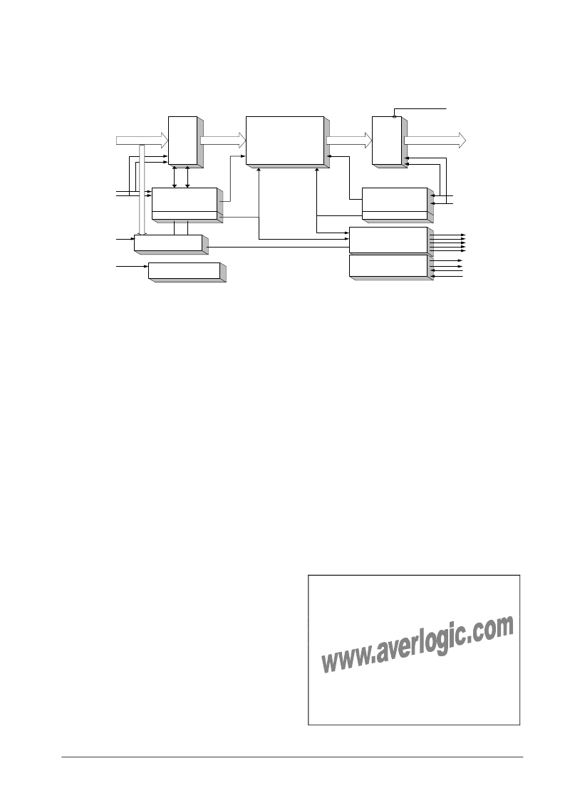
The 18bit input and output ports operate
independently at a maximum speed of 133
MHz. The built-in address decoder and
pointer
managing
straightforward bus interface to serially
read/write memory that reduces inter-chip
design efforts. The AL4CS2x5 embedded
memory array and high performance process
technologies
with
functions (read skip, fixed and programmable
status flags.. etc.) offer flexible memory
management.
These FIFOs support up to 18bit input and
output data bus-width that is controlled by
separate clock and enable signals respectively.
The input data is acquired at each rising edge
of a free running write clock while a write
enable control pin is asserted. The output data
is available after each rising edge of a free
running read clock while a read enable and
output enable control pins are asserted. When
output enable (/OE) is LOW, the data output
bus is active. If /OE is HIGH, the output data
bus will be in a high-impedance. This signal
can control whether the data is going to be
skipped during the read operation.
The
FIFO
Full/Empty,
programmable Almost Full/Almost Empty
flags are powerful functions that can help
circuits
provide
a
extended
controller
Half-Full
and
controlling software to manipulate the FIFO
more easily or to do retransmit operation.
Multiple AL4CS2x5s can cascade to expand
the storage depth or provide a longer delay.
The FIFOs can be chained by looping connect
/WXO, /RXO pins of the first FIFO chip to
/WXI, /RXI pins of successive chips
respectively and connect /WXO, /RXO pins of
last cascading chip to /WXI, /RXI pins of the
first FIFO chip. Expanding AL4CS2x5 data
bus width is also possible by using multiple
AL4CS2x5 chips in parallel.
These chips are available as a 64pin TQFP and
STQFP Package.
D
ISTRIBUTED BY
:
RAM ARRAY
256 x18, 512 x18
1024 x18, 2048 x18
4096 x18
Input
Buffer
Output
Buffer
Write Control
Logic
Read Control
Logic
Flag Logic
Expansion Logic
Write Pointer
Read Pointer
Offset Regissers
Reset Logic
Input data bus
Output data bus
/OE
WCLK
/WEN
/LD
/RS
RCLK
/REN
/FF
/EF
/PAF
/PAE
/WXO
/WXI
/RXI
AL4CS205/215/225/235/245 FIFO Block Diagram
相关PDF资料 |
PDF描述 |
|---|---|
| AL4CS225 | 256, 512, 1K, 2K, 4K x 18 Synchronous FIFOs |
| AL4CS235 | 256, 512, 1K, 2K, 4K x 18 Synchronous FIFOs |
| AL4CS245 | 256, 512, 1K, 2K, 4K x 18 Synchronous FIFOs |
| AL4CX263 | 16K/32K/64K/128K x9, 8K/16K/32K/64K x18 Synchronous FIFO |
| AL4CX273 | 16K/32K/64K/128K x9, 8K/16K/32K/64K x18 Synchronous FIFO |
相关代理商/技术参数 |
参数描述 |
|---|---|
| AL4CS221 | 制造商:未知厂家 制造商全称:未知厂家 功能描述:Synchronous FIFO |
| AL4CS225 | 制造商:AVERLOGIC 制造商全称:AVERLOGIC 功能描述:256, 512, 1K, 2K, 4K x 18 Synchronous FIFOs |
| AL4CS231 | 制造商:未知厂家 制造商全称:未知厂家 功能描述:Synchronous FIFO |
| AL4CS235 | 制造商:AVERLOGIC 制造商全称:AVERLOGIC 功能描述:256, 512, 1K, 2K, 4K x 18 Synchronous FIFOs |
| AL4CS241 | 制造商:未知厂家 制造商全称:未知厂家 功能描述:Synchronous FIFO |
发布紧急采购,3分钟左右您将得到回复。