- 您现在的位置:买卖IC网 > PDF目录18249 > ALD1116PAL (Advanced Linear Devices Inc)MOSFET 2N-CH 13.2V 4.8MA 8PDIP PDF资料下载
参数资料
| 型号: | ALD1116PAL |
| 厂商: | Advanced Linear Devices Inc |
| 文件页数: | 1/11页 |
| 文件大小: | 0K |
| 描述: | MOSFET 2N-CH 13.2V 4.8MA 8PDIP |
| 产品目录绘图: | 8-Pin Plastic Dip Package |
| 标准包装: | 50 |
| FET 型: | 2 个 N 沟道(双) |
| FET 特点: | 标准 |
| 漏极至源极电压(Vdss): | 13.2V |
| 电流 - 连续漏极(Id) @ 25° C: | 4.8mA |
| 开态Rds(最大)@ Id, Vgs @ 25° C: | 500 欧姆 @ 5V |
| Id 时的 Vgs(th)(最大): | 1V @ 1µA |
| 功率 - 最大: | 500mW |
| 安装类型: | 通孔 |
| 封装/外壳: | 8-DIP(0.300",7.62mm) |
| 供应商设备封装: | 8-PDIP |
| 包装: | 管件 |
| 其它名称: | 1014-1046 |
�� �
�
�A� DVANCED�
�L� INEAR�
�D� EVICES,� I� NC.�
�ALD1106/ALD1116�
�QUAD/DUAL� N-CHANNEL� MATCHED� PAIR� MOSFET� ARRAY�
�GENERAL� DESCRIPTION�
�APPLICATIONS�
�The� ALD1106/ALD1116� are� monolithic� quad/dual� N-channel� enhance-�
�ment� mode� matched� MOSFET� transistor� arrays� intended� for� a� broad� range�
�of� precision� analog� applications.� The� ALD1106/ALD1116� offer� high� input�
�impedance� and� negative� current� temperature� coefficient.� The� transistor�
�pairs� are� matched� for� minimum� offset� voltage� and� differential� thermal�
�response,� and� they� are� designed� for� precision� analog� switching� and�
�amplifying� applications� in� +2V� to� +12V� systems� where� low� input� bias�
�current,� low� input� capacitance� and� fast� switching� speed� are� desired.� These�
�MOSFET� devices� feature� very� large� (almost� infinite)� current� gain� in� a� low�
�frequency,� or� near� DC,� operating� environment.� The� ALD1106/ALD1116�
�?�
�?�
�?�
�?�
�?�
�?�
�?�
�?�
�Precision� current� mirrors�
�Precision� current� sources�
�Voltage� choppers�
�Differential� amplifier� input� stage�
�Voltage� comparator�
�Data� converters�
�Sample� and� Hold�
�Analog� signal� processing�
�are� building� blocks� for� differential� amplifier� input� stages,� transmission�
�gates,� and� multiplexer� applications,� current� sources� and� many� precision�
�analog� circuits.�
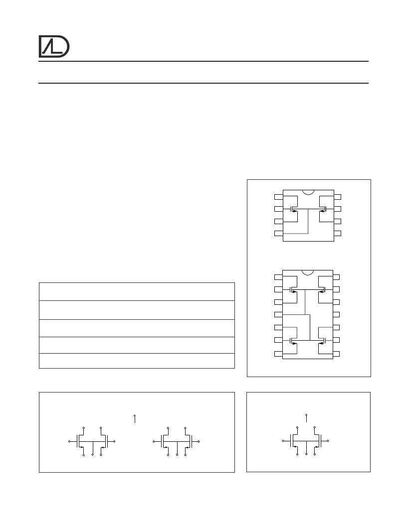
�PIN� CONFIGURATION�
�ALD1116�
�FEATURES�
�?� Low� threshold� voltage� of� 0.7V�
�?� Low� input� capacitance�
�?� Low� Vos� 2mV� typical�
�DN1�
�GN1�
�SN1�
�1�
�2�
�3�
�8�
�7�
�6�
�DN2�
�GN2�
�SN2�
�?� High� input� impedance� --� 10� 14� ?� typical�
�?� Negative� current� (I� DS� )� temperature� coefficient�
�?� Enhancement-mode� (normally� off)�
�?� DC� current� gain� 10� 9�
�?� Low� input� and� output� leakage� currents�
�V� -�
�4�
�TOP� VIEW�
�SAL,� PAL,� DA� PACKAGES�
�5�
�V� +�
�?� RoHS� compliant�
�ALD1106�
�ORDERING� INFORMATION� (“L”� suffix� denotes� lead-free� (RoHS))�
�DN1�
�1�
�14�
�DN2�
�0� °� C� to� +70� °� C�
�Operating� Temperature� Range*�
�0� °� C� to� +70� °� C� -55� °� C� to� +125� °� C�
�GN1�
�SN1�
�2�
�3�
�13�
�12�
�GN2�
�SN2�
�8-Pin� SOIC�
�8-Pin� Plastic� Dip�
�8-Pin� CERDIP�
�Package�
�ALD1116SAL�
�14-Pin� SOIC�
�Package�
�Package�
�ALD1116PAL�
�14-Pin� Plastic� Dip�
�Package�
�Package�
�ALD1116DA�
�14-Pin� CERDIP�
�Package�
�V� -�
�DN4�
�GN4�
�SN4�
�4�
�5�
�6�
�7�
�11�
�10�
�9�
�8�
�V� +�
�DN3�
�GN3�
�SN3�
�ALD1106SBL�
�ALD1106PBL�
�ALD1106DB�
�TOP� VIEW�
�SBL,� PBL,� DB� PACKAGES�
�*� Contact� factory� for� leaded� (non-RoHS)� or� high� temperature� versions.�
�BLOCK� DIAGRAM�
�ALD1106�
�V+� (11)�
�BLOCK� DIAGRAM�
�ALD1116�
�V+� (5)�
�D� N1� (1)�
�D� N2� (14)�
�~�
�D� N3� (10)�
�D� N4� (5)�
�D� N1� (1)�
�~�
�D� N2� (8)�
�G� N1� (2)�
�G� N2� (13)� G� N3� (9)�
�G� N4� (6)�
�G� N1� (2)�
�G� N2� (7)�
�S� N1� (3)�
�V-� (4)�
�S� N2� (12)�
�S� N3� (8)�
�V-� (4)�
�S� N4� (7)�
�S� N1� (3)�
�V-� (4)�
�S� N2� (6)�
�Rev� 2.1� ?2012� Advanced� Linear� Devices,� Inc.� 415� Tasman� Drive,� Sunnyvale,� CA� 94089-1706� Tel:� (408)� 747-1155� Fax:� (408)� 747-1286�
�www.aldinc.com�
�相关PDF资料 |
PDF描述 |
|---|---|
| MLW3022-00-PA-1A | SWITCH ROCKER DPDT 5A 125V |
| FXO-LC526R-25 | OSC 25 MHZ 2.5V LVDS SMD |
| ALD1115PAL | MOSFET N/P-CH 13.2V 8PDIP |
| JWL21BA1A-A | SWITCH ROCKER DPST 16A 125V |
| DC22.1111.111 | POWER ENTRY MOD W FILTER 1A |
相关代理商/技术参数 |
参数描述 |
|---|---|
| ALD1116SA | 功能描述:MOSFET Dual N-Channel Pair RoHS:否 制造商:STMicroelectronics 晶体管极性:N-Channel 汲极/源极击穿电压:650 V 闸/源击穿电压:25 V 漏极连续电流:130 A 电阻汲极/源极 RDS(导通):0.014 Ohms 配置:Single 最大工作温度: 安装风格:Through Hole 封装 / 箱体:Max247 封装:Tube |
| ALD1116SAL | 功能描述:MOSFET Dual N-Channel Pair RoHS:否 制造商:STMicroelectronics 晶体管极性:N-Channel 汲极/源极击穿电压:650 V 闸/源击穿电压:25 V 漏极连续电流:130 A 电阻汲极/源极 RDS(导通):0.014 Ohms 配置:Single 最大工作温度: 安装风格:Through Hole 封装 / 箱体:Max247 封装:Tube |
| ALD1117 | 制造商:ALD 制造商全称:Advanced Linear Devices 功能描述:DUAL N-CHANNEL AND DUAL P-CHANNEL MATCHED PAIR MOSFET |
| ALD1117DA | 制造商:ALD 制造商全称:Advanced Linear Devices 功能描述:QUAD/DUAL P-CHANNEL MATCHED MOSFET ARRAY |
| ALD1117PA | 功能描述:MOSFET Dual P-Channel Array RoHS:否 制造商:STMicroelectronics 晶体管极性:N-Channel 汲极/源极击穿电压:650 V 闸/源击穿电压:25 V 漏极连续电流:130 A 电阻汲极/源极 RDS(导通):0.014 Ohms 配置:Single 最大工作温度: 安装风格:Through Hole 封装 / 箱体:Max247 封装:Tube |
发布紧急采购,3分钟左右您将得到回复。