- 您现在的位置:买卖IC网 > PDF目录5894 > ALD1722SAL (Advanced Linear Devices Inc)IC OPAMP GP R-R CMOS 8SOIC PDF资料下载
参数资料
| 型号: | ALD1722SAL |
| 厂商: | Advanced Linear Devices Inc |
| 文件页数: | 4/9页 |
| 文件大小: | 0K |
| 描述: | IC OPAMP GP R-R CMOS 8SOIC |
| 标准包装: | 50 |
| 放大器类型: | 通用 |
| 电路数: | 1 |
| 输出类型: | 满摆幅 |
| 转换速率: | 2.8 V/µs |
| 增益带宽积: | 1.7MHz |
| 电流 - 输入偏压: | 0.01pA |
| 电压 - 输入偏移: | 25µV |
| 电流 - 电源: | 800µA |
| 电流 - 输出 / 通道: | 8mA |
| 电压 - 电源,单路/双路(±): | 4 V ~ 10 V,±2 V ~ 5 V |
| 工作温度: | 0°C ~ 70°C |
| 安装类型: | 表面贴装 |
| 封装/外壳: | 8-SOIC(0.154",3.90mm 宽) |
| 供应商设备封装: | 8-SOIC |
| 包装: | 管件 |
| 其它名称: | 1014-1096 |
ALD1722/ALD1722G
Advanced Linear Devices
4 of 9
Design & Operating Notes:
1. The ALD1722/ALD1722G CMOS operational amplifier uses a 3 gain
stage architecture and an improved frequency compensation scheme
to achieve large voltage gain, high output driving capability, and better
frequency stability. In a conventional CMOS operational amplifier
design, compensation is achieved with a pole splitting capacitor
together with a nulling resistor. This method is, however, very bias
dependent and thus cannot accommodate the large range of supply
voltage operation as is required from a stand alone CMOS operational
amplifier. The ALD1722/ALD1722G is internally compensated for
unity gain stability using a novel scheme that does not use a nulling
resistor. This scheme produces a clean single pole roll off in the gain
characteristics while providing for more than 70 degrees of phase
margin at the unity gain frequency. A unity gain buffer using the
ALD1722/ALD1722G will typically drive 400pF of external load ca-
pacitance without stability problems. In the inverting unity gain con-
figuration, it can drive up to 800pF of load capacitance. Compared to
other CMOS operational amplifiers, the ALD1722/ALD1722G has
shown itself to be more resistant to parasitic oscillations.
2. The ALD1722/ALD1722G has complementary p-channel and n-
channel input differential stages connected in parallel to accomplish
rail to rail input common mode voltage range. This means that with the
ranges of common mode input voltage close to the power supplies,
one of the two differential stages is switched off internally. To maintain
compatibility with other operational amplifiers, this switching point has
been selected to be about 1.5V above the negative supply voltage.
Since offset voltage trimming on the ALD1722/ALD1722G is made
when the input voltage is symmetrical to the supply voltages, this
internal switching does not affect a large variety of applications such
as an inverting amplifier or non-inverting amplifier with a gain larger
than 2.5 (5V operation), where the common mode voltage does not
make excursions below this switching point. The user should how-
ever, be aware that this switching does take place if the operational
amplifier is connected as a unity gain buffer and should make
provision in his design to allow for input offset voltage variations.
3. The input bias and offset currents are essentially input protection
diode reverse bias leakage currents, and are typically less than 1pA
at room temperature. This low input bias current assures that the
analog signal from the source will not be distorted by input bias
currents. Normally, this extremely high input impedance of greater
than 1014
would not be a problem as the source impedance would
limit the node impedance. However, for applications where source
impedance is very high, it may be necessary to limit noise and hum
pickup through proper shielding.
4. The output stage consists of class AB complementary output drivers,
capable of driving a low resistance load. The output voltage swing is
limited by the drain to source on-resistance of the output transistors
as determined by the bias circuitry, and the value of the load resistor.
When connected in the voltage follower configuration, the oscillation
resistant feature, combined with the rail to rail input and output feature,
makes an effective analog signal buffer for medium to high source
impedance sensors, transducers, and other circuit networks.
5. ALD1722/ALD1722G operational amplifier has been designed to
provide full static discharge protection. Internally, the design has been
carefully implemented to minimize latch up. However, care must be
exercised when handling the device to avoid strong static fields that
may degrade a diode junction, causing increased input leakage
currents. In using the operational amplifier, the user is advised to
power up the circuit before, or simultaneously with, any input voltages
applied and to limit input voltages to not exceed 0.3V of the power
supply voltage levels.
6. The ALD1722/ALD1722G has an internal design architecture that
provides robust high temperature operation. Contact factory for
custom screening versions.
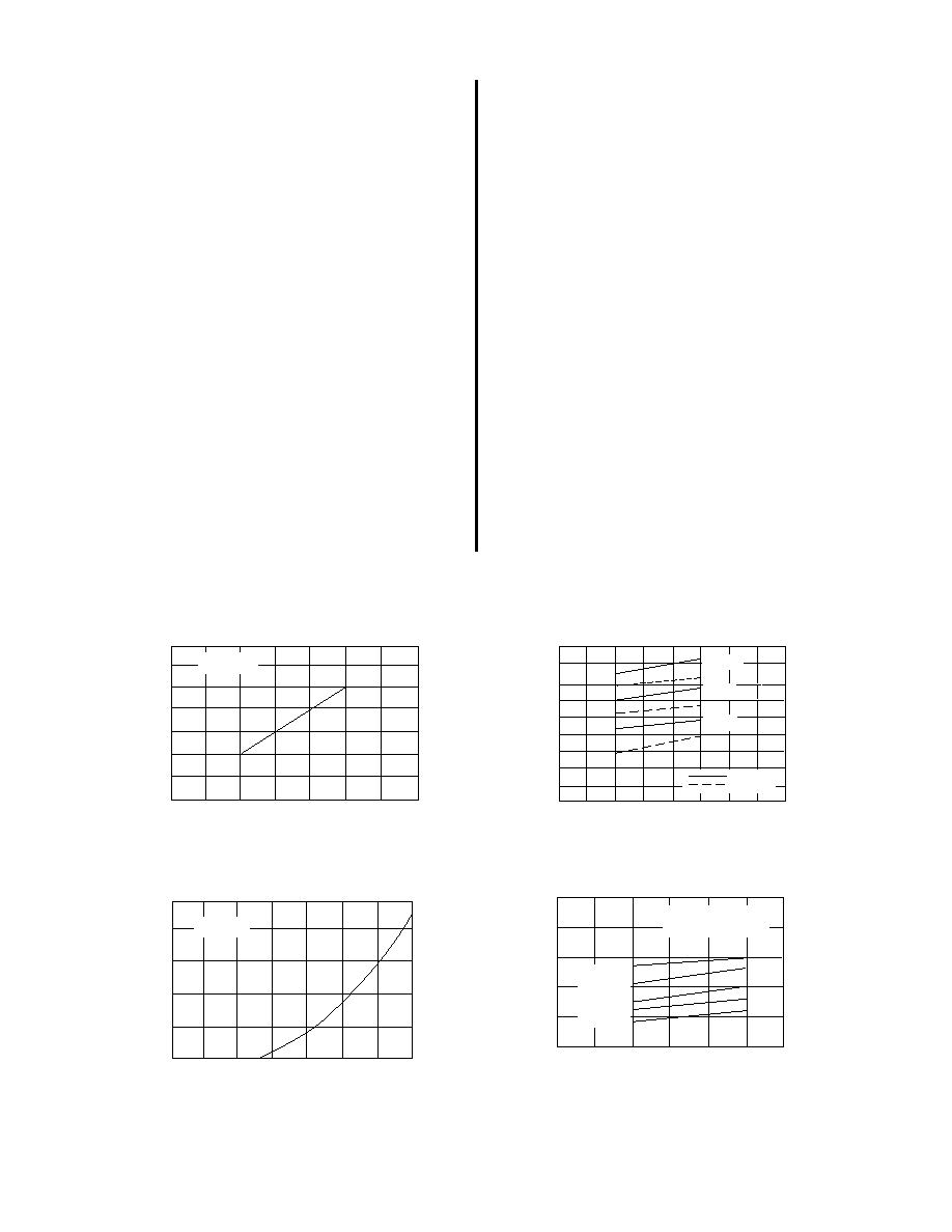
TYPICAL PERFORMANCE CHARACTERISTICS
INPUT BIAS CURRENT AS A FUNCTION
OF AMBIENT TEMPERATURE
AMBIENT TEMPERATURE (
°C)
100
10
1.0
0.01
0.1
INPUT
BIAS
CURRENT
(pA)
100
-25
0
75
125
50
25
-50
1000
VS = ±2.5V
COMMON MODE INPUT VOLTAGE RANGE
AS A FUNCTION OF SUPPLY VOLTAGE
SUPPLY VOLTAGE (V)
COMMON
MODE
INPUT
VOLTAGE
RANGE
(V)
±7
±6
±5
±4
±3
±2
±1
0
±1
±2
±3
±4
±5
±6
±7
TA = 25°C
0S
OPEN LOOP VOLTAGE GAIN AS A FUNCTION
OF SUPPLY VOLTAGE AND TEMPERATURE
SUPPLY VOLTAGE (V)
1000
100
10
1
OPEN
LOOP
VOLTAGE
GAIN
(V/mV)
0
±2
±4
±6
RL= 10K
RL= 5K
} -55
°C
} +25
°C
} +125
°C
±8
SUPPLY CURRENT AS A FUNCTION
OF SUPPLY VOLTAGE
SUPPLY VOLTAGE (V)
2.5
2.0
1.0
1.5
0
0.5
SUPPLY
CURRENT
(mA)
0
±1
±2
±3
±4
±5
±6
-25
°C
+25
°C
+80
°C
+125
°C
INPUTS GROUNDED
OUTPUT UNLOADED
TA = -55C
相关PDF资料 |
PDF描述 |
|---|---|
| LT6600IS8-20#TR | IC AMP DIFF LP FLTR 20MHZ 8-SOIC |
| 77315-101-05LF | BERGSTIK |
| RC0805FR-074R7L | RES 4.70 OHM 1/8W 1% 0805 SMD |
| LT6600IS8-2.5#TRPBF | IC AMP DIFF LP FLTR 2.5MHZ 8SOIC |
| 12FC | FUSE 12A 660V SEMI PROTECT BS88 |
相关代理商/技术参数 |
参数描述 |
|---|---|
| ALD1724EPAL | 功能描述:运算放大器 - 运放 EPAD(R) Hi-Slew Rate RoHS:否 制造商:STMicroelectronics 通道数量:4 共模抑制比(最小值):63 dB 输入补偿电压:1 mV 输入偏流(最大值):10 pA 工作电源电压:2.7 V to 5.5 V 安装风格:SMD/SMT 封装 / 箱体:QFN-16 转换速度:0.89 V/us 关闭:No 输出电流:55 mA 最大工作温度:+ 125 C 封装:Reel |
| ALD1724ESAL | 功能描述:运算放大器 - 运放 EPAD(R) Hi-Slew Rate RoHS:否 制造商:STMicroelectronics 通道数量:4 共模抑制比(最小值):63 dB 输入补偿电压:1 mV 输入偏流(最大值):10 pA 工作电源电压:2.7 V to 5.5 V 安装风格:SMD/SMT 封装 / 箱体:QFN-16 转换速度:0.89 V/us 关闭:No 输出电流:55 mA 最大工作温度:+ 125 C 封装:Reel |
| ALD1724PAL | 功能描述:运算放大器 - 运放 EPAD(R) Hi-Slew Rate RoHS:否 制造商:STMicroelectronics 通道数量:4 共模抑制比(最小值):63 dB 输入补偿电压:1 mV 输入偏流(最大值):10 pA 工作电源电压:2.7 V to 5.5 V 安装风格:SMD/SMT 封装 / 箱体:QFN-16 转换速度:0.89 V/us 关闭:No 输出电流:55 mA 最大工作温度:+ 125 C 封装:Reel |
| ALD1724SAL | 功能描述:运算放大器 - 运放 EPAD(R) Hi-Slew Rate RoHS:否 制造商:STMicroelectronics 通道数量:4 共模抑制比(最小值):63 dB 输入补偿电压:1 mV 输入偏流(最大值):10 pA 工作电源电压:2.7 V to 5.5 V 安装风格:SMD/SMT 封装 / 箱体:QFN-16 转换速度:0.89 V/us 关闭:No 输出电流:55 mA 最大工作温度:+ 125 C 封装:Reel |
| ALD1726 | 制造商:ALD 制造商全称:Advanced Linear Devices 功能描述:EPAD⑩ ULTRA MICROPOWER OPERATIONAL AMPLIFIER |
发布紧急采购,3分钟左右您将得到回复。