- 您现在的位置:买卖IC网 > PDF目录10735 > ALD2321APCL (Advanced Linear Devices Inc)IC COMP VOLT CMOS OUT DL 16PDIP PDF资料下载
参数资料
| 型号: | ALD2321APCL |
| 厂商: | Advanced Linear Devices Inc |
| 文件页数: | 4/11页 |
| 文件大小: | 0K |
| 描述: | IC COMP VOLT CMOS OUT DL 16PDIP |
| 标准包装: | 50 |
| 系列: | EPAD® |
| 类型: | 通用 |
| 元件数: | 2 |
| 输出类型: | CMOS,互补型,NMOS,开漏极,推挽式,TTL |
| 电压 - 电源,单路/双路(±): | 4 V ~ 10 V,±2 V ~ 5 V |
| 电压 - 输入偏移(最小值): | 0.2mV @ 5V |
| 电流 - 输入偏压(最小值): | 20pA @ 5V |
| 电流 - 静态(最大值): | 180µA |
| CMRR, PSRR(标准): | 80dB CMRR,75dB PSRR |
| 工作温度: | 0°C ~ 70°C |
| 封装/外壳: | 16-DIP(0.300",7.62mm) |
| 安装类型: | 通孔 |
| 包装: | 管件 |
| 其它名称: | 1014-1116 |
ALD2321A/ALD2321B/ALD2321
Advanced Linear Devices
2 of 11
Sink Output, can be connected together to form a push-pull output
which has the combined output capabilities of both channels.
In the dual complementary output mode, each comparator can be
used to drive separate loads. Due to the complementary nature of
the two outputs, only one output is active at any a given time, except
for a limited crossover time. When OUT (sink output) is active ON,
the OUT pin is sinking current and the OUTH pin is OFF and in high
impedance mode. Conversely, if OUTH pin is ON and sourcing
current, OUT pin is OFF. To configure push-pull output, simply
connect OUT (sink output) pin to OUTH pin.
Since each voltage comparator has its own complementary out-
puts, each comparator can be configured to have a different output
type. For example, one comparator output can be connected as
Open Drain output while the other comparator can be wired as
push-pull output. If used to drive capacitive loads, the output DC
current levels are at a very low level, at essentially leakage current
levels, which can be a power saving feature.
The ALD2321A/ALD2321B/ALD2321 can detect and resolve very
low voltage levels at high speed, with little or no overdrive voltage.
Compared with other voltage comparator devices that require 100
mV overdrive voltages, or multiple stage circuits that include input
preamp, etc., the ALD2321A/ALD2321B/ALD2321 can perform all
input to output functions in one device with minimal delay time and
with as low as a 1mV signal.
The ALD2321A/ALD2321B/ALD2321 is supplied with 4 external e-
trim pins, VE11, VE12, VE21, and VE22. These pins are used for
trimming of the voltage comparator offset voltages at the factory,
and normally should be left open unconnected. However, in some
cases these pins can be used as positive/negative feedback pins,
since these pins have a positive/negative factor on the offset
voltage. For example, see TYPICAL APPLICATIONS section
titled "Voltage Comparator With Output Feedback to Provide
Hysteresis."
GENERAL DESCRIPTION (cont'd)
In a printed circuit board layout, it is suggested that
these pins, along with no connect (N/C) pins 8 and 9,
be surrounded with ground traces to prevent any
possible crosstalk and noise coupling from other signal
sources.
Although not required for most applications, if neces-
sary, small valued capacitors of approximately 1000pF
can be mounted at these pins to ground to further
reduce noise. For information on customized trimming
under different biasing and power supply conditions,
please contact factory.
1
OUT1
COMPARATOR 1 SINK OUTPUT
OUTPUT
2
OUT1H
COMPARATOR 1 SOURCE OUTPUT
OUTPUT
3
-IN1
COMPARATOR 1 INVERTING INPUT
INPUT
4
+IN1
COMPARATOR 1 NON-INVERTING INPUT
INPUT
5
GND
GROUND / V- SUPPLY
-
6VE11
- VOS E-Trim COMPARATOR 1
INPUT
7VE12
+ VOS E-Trim COMPARATOR 1
INPUT
8
N/C
No Connect/Do Not connect externally
-
9
N/C
No Connect/Do Not connect externally
-
10
VE22
+VOS E-Trim COMPARATOR 2
INPUT
11
VE21
- VOS E-Trim COMPARATOR 2
INPUT
12
+IN2
COMPARATOR 2 NON-INVERTING INPUT
INPUT
13
-IN2
COMPARATOR 2 INVERTING INPUT
INPUT
14
OUT2H
COMPARATOR 2 SOURCE OUTPUT
OUTPUT
15
OUT2
COMPARATOR 2 SINK OUTPUT
OUTPUT
16
V+
V+ SUPPLY
-
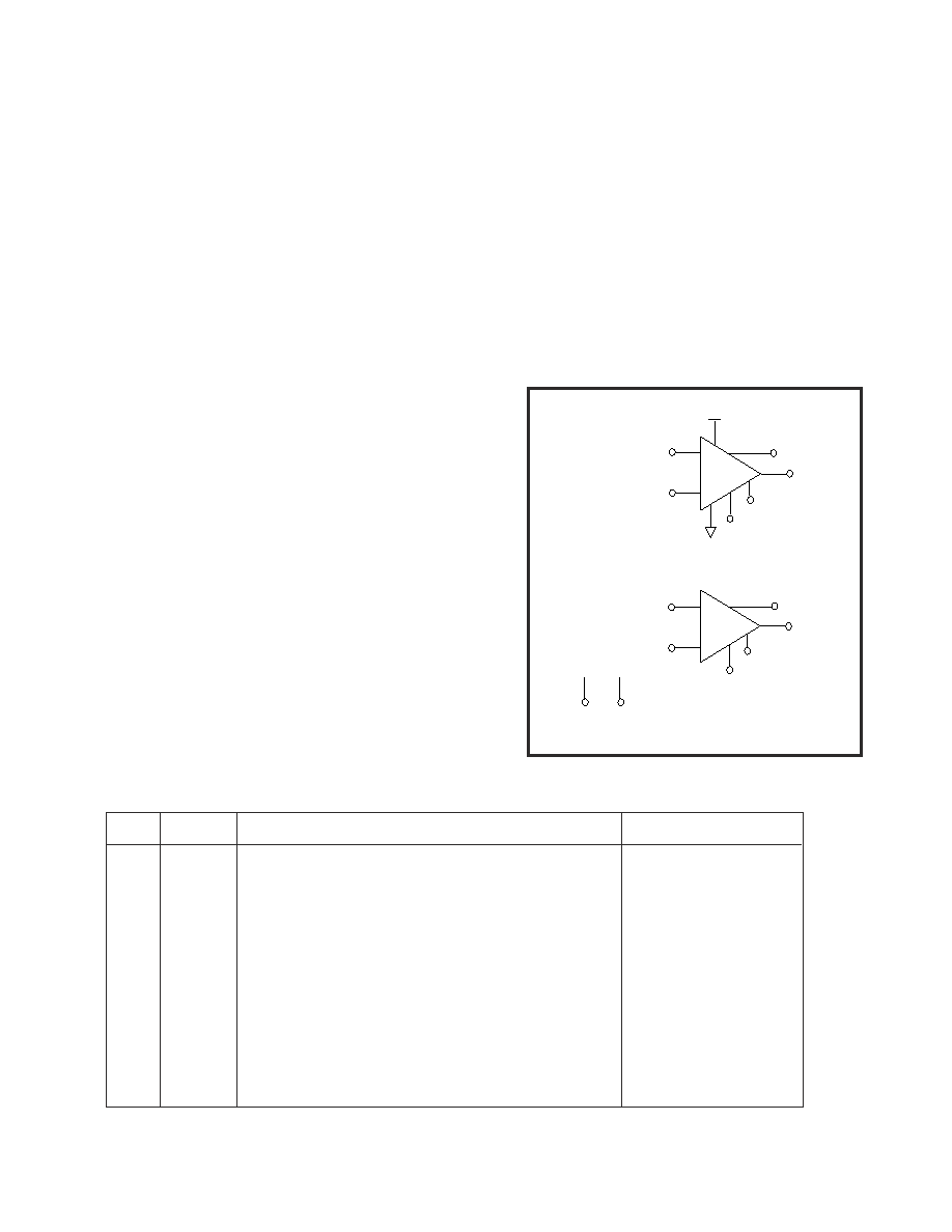
ALD2321 PIN IDENTIFICATION
PIN #
SYMBOL
FUNCTION
SIGNAL PROPAGATION
BLOCK DIAGRAM
(1) OUT1
NONINVERTING INPUT
+IN 1 (4)
INVERTING INPUT
-IN 1 (3)
(16) V+
(2) OUT1H
VE11
GND
(6)
(7) VE12
(5)
(15) OUT2
VE21
INVERTING INPUT
-IN 2 (13)
(14) OUT2H
VE22
(11)
(10)
N/C
(8)
(9)
N/C
NONINVERTING INPUT
+IN 2 (12)
-
+
-
+
相关PDF资料 |
PDF描述 |
|---|---|
| VI-2N2-IW | CONVERTER MOD DC/DC 15V 100W |
| ALD4302PBL | IC COMP VOLT PUSH-PULL QD 14PDIP |
| ALD4303PBL | IC COMP VOLT CMOS OD QUAD 14PDIP |
| VI-2N2-CV-B1 | CONVERTER MOD DC/DC 15V 150W |
| ALD2301BSAL | IC COMP VOLT CMOS OD DUAL 8SOIC |
相关代理商/技术参数 |
参数描述 |
|---|---|
| ALD2321ASC | 功能描述:校验器 IC .2mV Prec Dual with Comp Output Drivers RoHS:否 制造商:STMicroelectronics 产品: 比较器类型: 通道数量: 输出类型:Push-Pull 电源电压-最大:5.5 V 电源电压-最小:1.1 V 补偿电压(最大值):6 mV 电源电流(最大值):1350 nA 响应时间: 最大工作温度:+ 125 C 安装风格:SMD/SMT 封装 / 箱体:SC-70-5 封装:Reel |
| ALD2321ASCL | 功能描述:校验器 IC .2mV Prec Dual with Comp Output Drivers RoHS:否 制造商:STMicroelectronics 产品: 比较器类型: 通道数量: 输出类型:Push-Pull 电源电压-最大:5.5 V 电源电压-最小:1.1 V 补偿电压(最大值):6 mV 电源电流(最大值):1350 nA 响应时间: 最大工作温度:+ 125 C 安装风格:SMD/SMT 封装 / 箱体:SC-70-5 封装:Reel |
| ALD2321B | 制造商:ALD 制造商全称:Advanced Linear Devices 功能描述:ULTRA LOW VOS EPAD DUAL CMOS ANALOG VOLTAGE COMPARATOR |
| ALD2321BDC | 制造商:ALD 制造商全称:Advanced Linear Devices 功能描述:ULTRA LOW VOS EPAD DUAL CMOS ANALOG VOLTAGE COMPARATOR |
| ALD2321BPC | 功能描述:校验器 IC .5mV Prec Dual with Comp Output Drivers RoHS:否 制造商:STMicroelectronics 产品: 比较器类型: 通道数量: 输出类型:Push-Pull 电源电压-最大:5.5 V 电源电压-最小:1.1 V 补偿电压(最大值):6 mV 电源电流(最大值):1350 nA 响应时间: 最大工作温度:+ 125 C 安装风格:SMD/SMT 封装 / 箱体:SC-70-5 封装:Reel |
发布紧急采购,3分钟左右您将得到回复。