- 您现在的位置:买卖IC网 > PDF目录5888 > ALD2704ASAL (Advanced Linear Devices Inc)IC OPAMP GP R-R CMOS DUAL 8SOIC PDF资料下载
参数资料
| 型号: | ALD2704ASAL |
| 厂商: | Advanced Linear Devices Inc |
| 文件页数: | 1/9页 |
| 文件大小: | 0K |
| 描述: | IC OPAMP GP R-R CMOS DUAL 8SOIC |
| 标准包装: | 50 |
| 放大器类型: | 通用 |
| 电路数: | 2 |
| 输出类型: | 推挽式,满摆幅 |
| 转换速率: | 5 V/µs |
| 增益带宽积: | 2.1MHz |
| 电流 - 输入偏压: | 1pA |
| 电压 - 输入偏移: | 1000µV |
| 电流 - 电源: | 5mA |
| 电流 - 输出 / 通道: | 15mA |
| 电压 - 电源,单路/双路(±): | 6.5 V ~ 12 V,±3.25 V ~ 6 V |
| 工作温度: | 0°C ~ 70°C |
| 安装类型: | 表面贴装 |
| 封装/外壳: | 8-SOIC(0.154",3.90mm 宽) |
| 供应商设备封装: | 8-SOIC |
| 包装: | 管件 |
| 其它名称: | 1014-1138 |
Rev 2.0 2010 Advanced Linear Devices, Inc. 415 Tasman Drive, Sunnyvale, CA 94089-1706 Tel: (408) 747-1155 Fax: (408) 747-1286
www.aldinc.com
DUAL RAIL-TO-RAIL CMOS OPERATIONAL AMPLIFIER
ALD2704A/ALD2704B
ALD2704
ADVANCED
LINEAR
DEVICES, INC.
Operating Temperature Range
0°C to +70°C0°C to +70°C
-55°C to 125°C
8-Pin
Small Outline
Plastic Dip
CERDIP
Package (SOIC)
Package
ALD2704ASAL
ALD2704APAL
ALD2704ADA
ALD2704BSAL
ALD2704BPAL
ALD2704BDA
ALD2704SAL
ALD2704PAL
ALD2704DA
* Contact factory for leaded (non-RoHS) or high temperature versions.
ORDERING INFORMATION (“L” suffix denotes lead-free (RoHS))
GENERAL DESCRIPTION
The ALD2704A/ALD2704B/ALD2704 is a dual monolithic operational
amplifier with MOSFET input that has rail-to-rail input and output voltage
ranges. The input voltage range and output voltage range are very close
to the positive and negative power supply voltages. Typically the input
voltage can be beyond positive power supply voltage V+ or the negative
power supply voltage V- by up to 300mV. The output voltage swings to
within 60mV of either positive or negative power supply voltages at rated
load.
With high impedance load, the output voltage of the ALD2704A/ALD2704B/
ALD2704 approaches within 1mV of the power supply rails. This device
is designed as an alternative to the popular J-FET input operational
amplifier in applications where lower operating voltages, such as 9V
battery or ±3.25V to ±5V power supplies are being used. The ALD2704A/
ALD2704B/ALD2704 offers high slew rate of 5V/s. It is designed and
manufactured with Advanced Linear Devices' standard enhanced ACMOS
silicon gate CMOS process, and it offers low unit cost and exceptional
reliability.
The rail-to-rail input and output feature of the ALD2704A/ALD2704B/
ALD2704 expands signal voltage range for a given operating supply
voltage and allows numerous analog serial stages to be implemented
without losing operating voltage margin. The output stage is designed to
drive up to 10mA into 400pF capacitive and 1.5K resistive loads at unity
gain and up to 4000pF at a gain of 5. Short circuit protection to either
ground or the power supply rails is at approximately 15mA clamp current.
Due to complementary output stage design, the output can source and
sink 10mA into a load with symmetrical drive and is ideally suited for
applications where push-pull voltage drive is desired.
For each of the operational amplifier, the offset voltage is trimmed on-chip
to eliminate the need for external nulling in many applications.
For
precision applications, the output is designed to settle to 0.1% in 2s. In
large signal buffer applications, the operational amplifier can function as
an ultrahigh input impedance voltage follower /buffer that allows input and
output voltage swings from positive to negative supply voltages. This
feature is intended to greatly simplify systems design and eliminate higher
voltage power supplies in many applications. Additionally, robust design
and rigorous screening make this device especially suitable for operation
in temperature-extreme environments and rugged conditions.
FEATURES
Rail-to-rail input and output voltage ranges
Symmetrical push-pull output drives
Output settles to 2mV of supply rails
5.0V/s slew rate
High capacitive load capability -- up to 4000pF
No frequency compensation required -- unity
gain stable
Extremely low input bias currents -- <1.0pA
typical (20pA max.)
Ideal for high source impedance applications
High voltage gain -- typically 100V/mV
Output short circuit protected
Unity gain bandwidth of 2.1MHz
Suitable for rugged, temperature-extreme
environments
APPLICATIONS
Voltage amplifier
Voltage follower/buffer
Charge integrator
Photodiode amplifier
Data acquisition systems
High performance portable instruments
Signal conditioning circuits
Low leakage amplifiers
Active filters
Sample/Hold amplifier
Picoammeter
Current to voltage converter
Coaxial cable driver
Capacitive sensor amplifier
Piezoelectric transducer amplifier
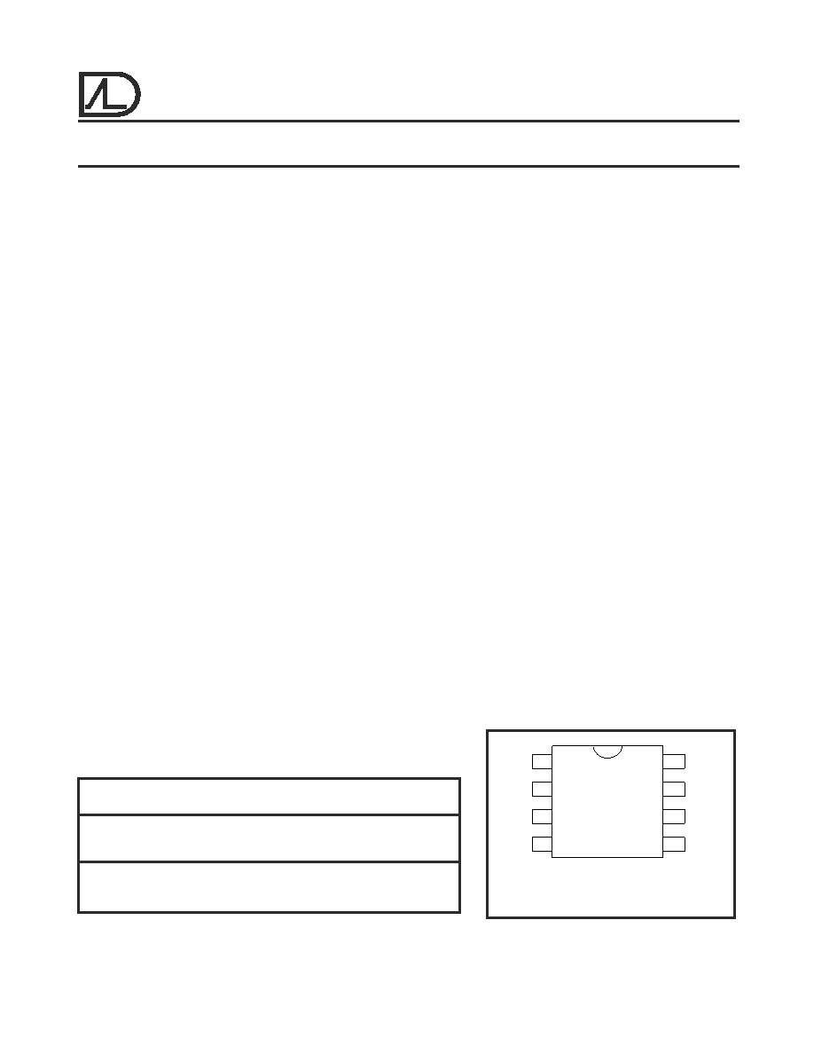
PIN CONFIGURATION
TOP VIEW
SAL, PAL, DA PACKAGES
1
2
3
4
8
7
6
5
OUT A
-IN A
+IN A
V+
-IN B
+IN B
V -
OUT B
相关PDF资料 |
PDF描述 |
|---|---|
| RC0805FR-073R16L | RES 3.16 OHM 1/8W 1% 0805 SMD |
| TSW-147-08-G-D | CONN HEADER 94POS .100" DL GOLD |
| LT1168CN8 | IC AMP INSTR PROG PREC LP 8DIP |
| 16LET | FUSE 16A 240V TYPE T FUSE BRITSH |
| ALD2702APAL | IC OPAMP GP R-R CMOS DUAL 8PDIP |
相关代理商/技术参数 |
参数描述 |
|---|---|
| ALD2704B | 制造商:ALD 制造商全称:Advanced Linear Devices 功能描述:DUAL RAIL-TO-RAIL CMOS OPERATIONAL AMPLIFIER |
| ALD2704BDA | 制造商:未知厂家 制造商全称:未知厂家 功能描述:Operational Amplifier |
| ALD2704BPA | 功能描述:运算放大器 - 运放 High Slew Rate RoHS:否 制造商:STMicroelectronics 通道数量:4 共模抑制比(最小值):63 dB 输入补偿电压:1 mV 输入偏流(最大值):10 pA 工作电源电压:2.7 V to 5.5 V 安装风格:SMD/SMT 封装 / 箱体:QFN-16 转换速度:0.89 V/us 关闭:No 输出电流:55 mA 最大工作温度:+ 125 C 封装:Reel |
| ALD2704BPAL | 功能描述:运算放大器 - 运放 5V 2.0mV Dual Prec Rail-to-Rail RoHS:否 制造商:STMicroelectronics 通道数量:4 共模抑制比(最小值):63 dB 输入补偿电压:1 mV 输入偏流(最大值):10 pA 工作电源电压:2.7 V to 5.5 V 安装风格:SMD/SMT 封装 / 箱体:QFN-16 转换速度:0.89 V/us 关闭:No 输出电流:55 mA 最大工作温度:+ 125 C 封装:Reel |
| ALD2704BSA | 功能描述:运算放大器 - 运放 High Slew Rate RoHS:否 制造商:STMicroelectronics 通道数量:4 共模抑制比(最小值):63 dB 输入补偿电压:1 mV 输入偏流(最大值):10 pA 工作电源电压:2.7 V to 5.5 V 安装风格:SMD/SMT 封装 / 箱体:QFN-16 转换速度:0.89 V/us 关闭:No 输出电流:55 mA 最大工作温度:+ 125 C 封装:Reel |
发布紧急采购,3分钟左右您将得到回复。