- 您现在的位置:买卖IC网 > PDF目录5688 > ALD4706ASBL (Advanced Linear Devices Inc)IC OPAMP GP R-R CMOS QUAD 14SOIC PDF资料下载
参数资料
| 型号: | ALD4706ASBL |
| 厂商: | Advanced Linear Devices Inc |
| 文件页数: | 1/9页 |
| 文件大小: | 0K |
| 描述: | IC OPAMP GP R-R CMOS QUAD 14SOIC |
| 标准包装: | 56 |
| 放大器类型: | 通用 |
| 电路数: | 4 |
| 输出类型: | 满摆幅 |
| 转换速率: | 0.17 V/µs |
| 增益带宽积: | 200kHz |
| 电流 - 输入偏压: | 0.1pA |
| 电压 - 输入偏移: | 2000µV |
| 电流 - 电源: | 120µA |
| 电流 - 输出 / 通道: | 200µA |
| 电压 - 电源,单路/双路(±): | 2 V ~ 12 V,±1 V ~ 6 V |
| 工作温度: | 0°C ~ 70°C |
| 安装类型: | 表面贴装 |
| 封装/外壳: | 14-SOIC(0.154",3.90mm 宽) |
| 供应商设备封装: | 14-SOIC |
| 包装: | 管件 |
Rev 2.0 2010 Advanced Linear Devices, Inc. 415 Tasman Drive, Sunnyvale, CA 94089-1706 Tel: (408) 747-1155 Fax: (408) 747-1286
www.aldinc.com
DUAL ULTRA MICROPOWER RAIL-TO-RAIL CMOS OPERATIONAL AMPLIFIER
ALD4706A/ALD4706B
ALD4706
ADVANCED
LINEAR
DEVICES, INC.
Operating Temperature Range
0°C to +70°C0°C to +70°C
-55°C to 125°C
14-Pin
Small Outline
Plastic Dip
CERDIP
Package (SOIC)
Package
ALD4706ASBL
ALD4706APBL
ALD4706ADB
ALD4706BSBL
ALD4706BPBL
ALD4706BDB
ALD4706SBL
ALD4706PBL
ALD4706DB
* Contact factory for leaded (non-RoHS) or high temperature versions.
ORDERING INFORMATION (“L” suffix denotes lead-free (RoHS))
GENERAL DESCRIPTION
The ALD4706A/ALD4706B/ALD4706 is a quad monolithic CMOS ultra
micropower high slew-rate operational amplifier intended for a broad
range of analog applications using ±1V to ±5V dual power supply
systems, as well as +2V to +10V battery operated systems. All device
characteristics are specified for +5V single supply or ±2.5V dual supply
systems. Total supply current for four operational amplifiers is 200A
maximum at 5V supply voltage. It is manufactured with Advanced Linear
Devices' enhanced ACMOS silicon gate CMOS process.
The ALD4706A/ALD4706B/ALD4706 is designed to offer a trade-off of
performance parameters providing a wide range of desired specifications.
It has been developed specifically for the +5V single supply or ±1V to
±5V dual supply user and offers the popular industry standard pin
configuration of LM324 types and ICL7641 types.
Several important characteristics of the device make application easier
to implement at these voltages. First, each operational amplifier can
operate with rail-to-rail input and output voltages. This means the signal
input voltage and output voltage can be equal to or near to the positive
and negative supply voltages. This feature allows numerous analog
serial stages and flexibility in input signal bias levels. Second, each
device was designed to accommodate mixed applications where digital
and analog circuits may operate off the same power supply or battery.
Third, the output stage can typically drive up to 25pF capacitive and
20K resistive loads. These features, combined with extremely low
input currents, high open loop voltage gain of 100V/mV, useful bandwidth
of 200KHz, a slew rate of 0.17V/s, low power dissipation of 0.5mW,
low offset voltage and temperature drift, make the ALD4706A/ALD4706B/
ALD4706 a versatile, ultra micropower quad operational amplifier.
The ALD4706A/ALD4706B/ALD4706, designed and fabricated with
silicon gate CMOS technology, offers 0.1pA typical input bias current.
Due to low voltage and low power operation, reliability and operating
characteristics, such as input bias currents and warm up time, are greatly
improved. Additionally, robust design and rigorous screening make this
device especially suitable for operation in temperature-extreme
environments and rugged conditions.
APPLICATIONS
Voltage follower/buffer/amplifier
Charge integrator
Photodiode amplifier
Data acquisition systems
High performance portable instruments
Signal conditioning circuits
Sensor and transducer amplifiers
Low leakage amplifiers
Active filters
Sample/Hold amplifier
Picoammeter
Current to voltage converter
FEATURES
All parameters specified for + 5V single
supply or ± 2.5V dual supply systems
Rail- to- rail input and output voltage ranges
Unity gain stable
Extremely low input bias currents -- 0.1pA
High source impedance applications
Dual power supply ±1.0V to ±5.0V
Single power supply +2V to +10V
High voltage gain
Output short circuit protected
Unity gain bandwidth of 0.2MHz
Slew rate of 0.17V/s
Power dissipation of 20A per op amp
Symmetrical output drive
Suitable for rugged, temperature-extreme
environments
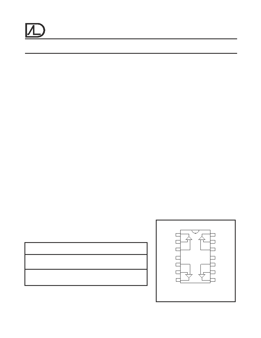
PIN CONFIGURATION
TOP VIEW
SBL, PBL, DB PACKAGES
OUT D
-IN D
+IN D
V-
+IN C
-IN C
OUT C
OUT A
-IN A
+IN A
V+
+IN B
-IN B
OUT B
1
2
3
4
5
6
7
8
9
10
11
12
13
14
相关PDF资料 |
PDF描述 |
|---|---|
| 95736-412 | CLINCHER R/A LATCHING HEADER |
| 78207-222HLF | FRICTION LATCH HEADER DR R/A |
| 5535034-5 | CONN RCPT 48POS EUROCARD C/2 |
| 165172-2 | CONN PIN WIRE 16-14AWG TIN PIDG |
| 79257-272HLF | BERGSTIK II DR R/A WIDE BODY |
相关代理商/技术参数 |
参数描述 |
|---|---|
| ALD4706ASF | 制造商:未知厂家 制造商全称:未知厂家 功能描述:Analog IC |
| ALD4706B | 制造商:ALD 制造商全称:Advanced Linear Devices 功能描述:QUAD ULTRA MICROPOWER RAIL-TO-RAIL CMOS OPERATIONAL AMPLIFIER |
| ALD4706BDB | 制造商:ALD 制造商全称:Advanced Linear Devices 功能描述:Operational Amplifier |
| ALD4706BPB | 功能描述:运算放大器 - 运放 Ultra-Micropower RoHS:否 制造商:STMicroelectronics 通道数量:4 共模抑制比(最小值):63 dB 输入补偿电压:1 mV 输入偏流(最大值):10 pA 工作电源电压:2.7 V to 5.5 V 安装风格:SMD/SMT 封装 / 箱体:QFN-16 转换速度:0.89 V/us 关闭:No 输出电流:55 mA 最大工作温度:+ 125 C 封装:Reel |
| ALD4706BPBL | 功能描述:运算放大器 - 运放 Quad Ultra-Micropowr RoHS:否 制造商:STMicroelectronics 通道数量:4 共模抑制比(最小值):63 dB 输入补偿电压:1 mV 输入偏流(最大值):10 pA 工作电源电压:2.7 V to 5.5 V 安装风格:SMD/SMT 封装 / 箱体:QFN-16 转换速度:0.89 V/us 关闭:No 输出电流:55 mA 最大工作温度:+ 125 C 封装:Reel |
发布紧急采购,3分钟左右您将得到回复。