- 您现在的位置:买卖IC网 > PDF目录378310 > AM26LS32 (Motorola, Inc.) QUAD EIA-422/3 LINE RECEIVER WITH THREE.STATE OUTPUTS PDF资料下载
参数资料
| 型号: | AM26LS32 |
| 厂商: | Motorola, Inc. |
| 英文描述: | QUAD EIA-422/3 LINE RECEIVER WITH THREE.STATE OUTPUTS |
| 中文描述: | 四环境影响评估,3分之422线路接收器输出与THREE.STATE |
| 文件页数: | 2/4页 |
| 文件大小: | 81K |
| 代理商: | AM26LS32 |
AM26LS32
2
MOTOROLA ANALOG IC DEVICE DATA
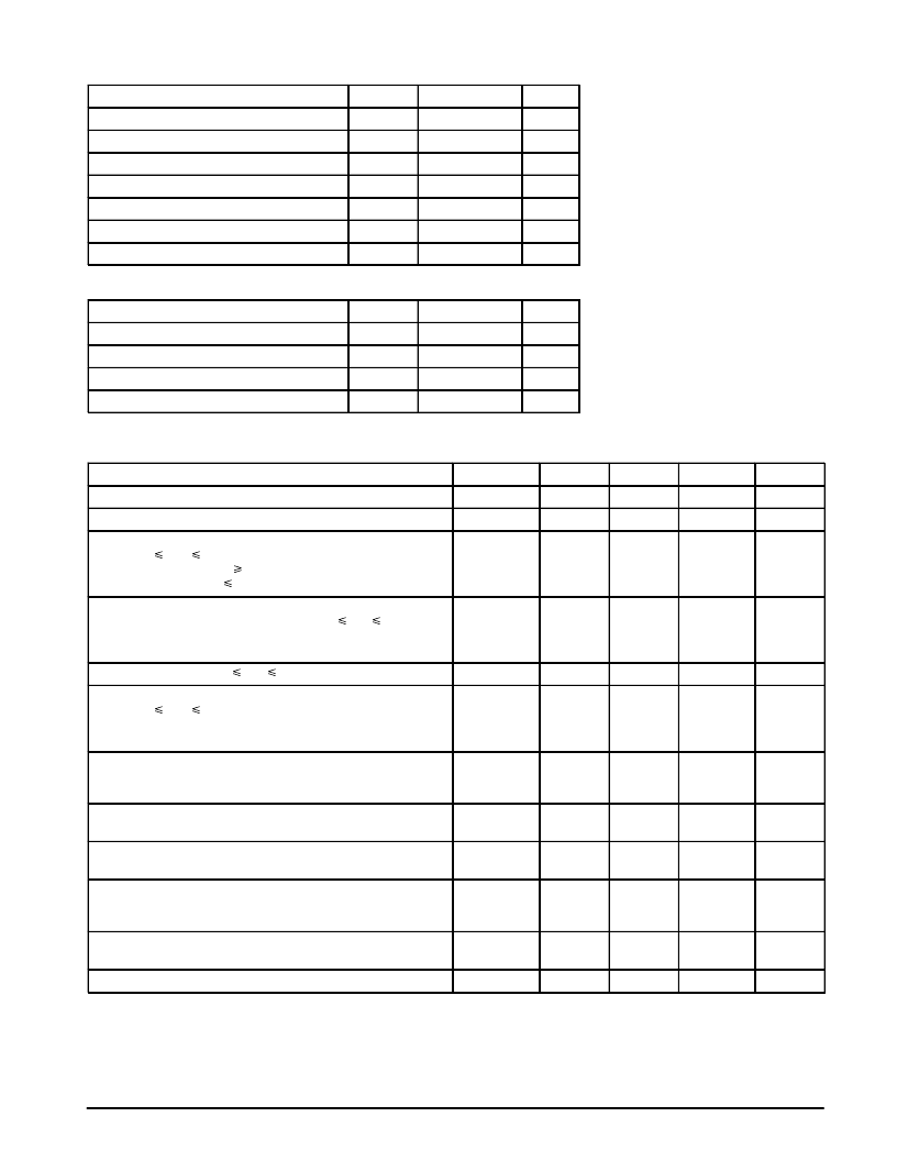
MAXIMUM RATINGS
Rating
Symbol
Value
Unit
Power Supply Voltage
VCC
VICM
VID
VI
IO
Tstg
TJ
7.0
Vdc
Input Common Mode Voltage
±
25
Vdc
Input Differential Voltage
±
25
Vdc
Three–State Control Input Voltage
7.0
Vdc
Output Sink Current
50
mA
Storage Temperature
– 65 to + 150
°
C
Operating Junction Temperature
+ 150
°
C
RECOMMENDED OPERATING CONDITIONS
Rating
Symbol
Value
Unit
Power Supply Voltage
VCC
TA
VICR
VIDR
4.75 to 5.25
Vdc
Operating Ambient Temperature
0 to + 70
°
C
Input Common Mode Voltage Range
– 7.0 to + 7.0
Vdc
Input Differential Voltage Range
6.0
Vdc
ELECTRICAL CHARACTERISTICS
(Unless otherwise noted, minimum and maximum limits apply over recommended temperature
and power supply voltage ranges. Typical values are for TA = 25
°
C, VCC = 5.0 V and VIC = 0 V. See Note 1.)
Characteristic
Symbol
Min
Typ
Max
Unit
Input Voltage – High Logic State (Three–State Control)
VIH
VIL
2.0
–
–
V
Input Voltage – Low Logic State (Three–State Control)
–
–
0.8
V
Differential Input Threshold Voltage (Note 2)
(–7.0 V
VIC
7.0 V, VIH = 2.0 V)
(IO = –0.4 mA, VOH
(IO = 8.0 mA, VOL
2.7 V)
0.45 V)
VTH(D)
–
–
–
–
0.2
–0.2
V
Input Bias Current
(VCC = 0 V or 5.25) (Other Inputs at –15 V
Vin = +15 V
Vin = –15 V
Vin
+15 V)
IIB(D)
–
–
–
–
2.3
–2.8
mA
Input Resistance ( –15 V
Vin
+15 V)
Rin
6.0 K
–
–
Ohms
Input Balance and Output Level
(–7.0 V
VIC
(IO = –0.4 mA, VID = 0.4 V)
(IO = 8.0 mA, VID = –0.4 V)
7.0 V, VIH = 2.0 V, See Note 3)
VOH
VOL
2.7
–
–
–
–
0.45
V
Output Third State Leakage Current
(VI(D) = + 3.0 V, VIL = 0.8 V, VO = 0.4 V)
(VI(D) = – 3.0 V, VIL = 0.8 V, VO = 2.4 V)
IOZ
–
–
–
–
–20
20
μ
A
Output Short Circuit Current
(VI(D) = 3.0 V, VIH = 2.0 V, VO = 0 V, See Note 4)
IOS
–15
–
–85
mA
Input Current – Low Logic State (Three–State Control)
(VIL = 0.4 V)
IIL
–
–
–360
μ
A
Input Current – High Logic State (Three–State Control)
(VIH = 2.7 V)
(VIH = 5.5 V)
IIH
–
–
–
–
20
100
μ
A
Input Clamp Diode Voltage (Three–State Control)
(IIC = –18 mA)
VIK
–
–
–1.5
V
Power Supply Current (VIL = 0 V) (All Inputs Grounded)
ICC
–
–
70
mA
NOTES:
1.All currents into device pins are shown as positive, out of device pins are negative. All voltages referenced to ground unless otherwise noted.
2.Differential input threshold voltage and guaranteed output levels are done simultaneously for worst case.
3.Refer to EIA–422/3 for exact conditions. Input balance and guaranteed output levels are done simultaneously for worst case.
4.Only one output at a time should be shorted.
相关PDF资料 |
PDF描述 |
|---|---|
| AM3341 | 64 x 4 BITS FIRST-IN FIRST-OUT MEMORIES |
| AM2841 | 64 x 4 BITS FIRST-IN FIRST-OUT MEMORIES |
| AM2841A | 64 x 4 BITS FIRST-IN FIRST-OUT MEMORIES |
| AM2841ADC | 64 x 4 BITS FIRST-IN FIRST-OUT MEMORIES |
| AM2841APC | 64 x 4 BITS FIRST-IN FIRST-OUT MEMORIES |
相关代理商/技术参数 |
参数描述 |
|---|---|
| AM26LS32/B2A | 制造商:未知厂家 制造商全称:未知厂家 功能描述:Line Receiver |
| AM26LS32/B2C | 制造商: 功能描述: 制造商:undefined 功能描述: |
| AM26LS32/BEA | 制造商:Advanced Micro Devices 功能描述: 制造商:Advanced Micro Devices 功能描述:Line Receiver, Quad, Differential, 16 Pin, Ceramic, DIP |
| AM26LS32/BFA | 制造商:未知厂家 制造商全称:未知厂家 功能描述:Line Receiver |
| AM26LS32A | 制造商:TI 制造商全称:Texas Instruments 功能描述:QUADRUPLE DIFFERENTIAL LINE RECEIVERS |
发布紧急采购,3分钟左右您将得到回复。