- 您现在的位置:买卖IC网 > PDF目录375300 > AM29F010B70PE (Spansion Inc.) 1 Megabit (128 K x 8-bit) CMOS 5.0 Volt-only, Uniform Sector Flash Memory PDF资料下载
参数资料
| 型号: | AM29F010B70PE |
| 厂商: | Spansion Inc. |
| 英文描述: | 1 Megabit (128 K x 8-bit) CMOS 5.0 Volt-only, Uniform Sector Flash Memory |
| 中文描述: | 1兆位(128亩× 8位)的CMOS 5.0伏只,统一部门快闪记忆体 |
| 文件页数: | 14/35页 |
| 文件大小: | 849K |
| 代理商: | AM29F010B70PE |
第1页第2页第3页第4页第5页第6页第7页第8页第9页第10页第11页第12页第13页当前第14页第15页第16页第17页第18页第19页第20页第21页第22页第23页第24页第25页第26页第27页第28页第29页第30页第31页第32页第33页第34页第35页
November 18, 2002
Am29F010B
13
Note:
See the appropriate Command Definitions table for
program command sequence.
Figure 1.
Program Operation
Chip Erase Command Sequence
Chip erase is a six-bus-cycle operation. The chip erase
command sequence is initiated by writing two unlock
cycles, followed by a set-up command. Two additional
unlock write cycles are then followed by the chip erase
command, which in turn invokes the Embedded Erase
algorithm. The device does
not
require the system to
preprogram prior to erase. The Embedded Erase algo-
rithm automatically preprograms and verifies the entire
memory for an all zero data pattern prior to electrical
erase. The system is not required to provide any con-
trols or timings during these operations. The Command
Definitions table shows the address and data require-
ments for the chip erase command sequence.
Any commands written to the chip during the Embed-
ded Erase algorithm are ignored.
The system can determine the status of the erase op-
eration by using DQ7 or DQ6. See “Write Operation
Status” for information on these status bits. When the
Embedded Erase algorithm is complete, the device re-
turns to reading array data and addresses are no
longer latched.
Figure 2 illustrates the algorithm for the erase opera-
tion. See the Erase/Program Operations tables in “AC
Characteristics” for parameters, and to the Chip/Sector
Erase Operation Timings for timing waveforms.
Sector Erase Command Sequence
Sector erase is a six bus cycle operation. The sector
erase command sequence is initiated by writing two
unlock cycles, followed by a set-up command. Two ad-
ditional unlock write cycles are then followed by the
address of the sector to be erased, and the sector
erase command. The Command Definitions table
shows the address and data requirements for the sec-
tor erase command sequence.
The device does
not
require the system to preprogram
the memory prior to erase. The Embedded Erase algo-
rithm automatically programs and verifies the sector for
an all zero data pattern prior to electrical erase. The
system is not required to provide any controls or tim-
ings during these operations.
After the command sequence is written, a sector erase
time-out of 50 μs begins. During the time-out period,
additional sector addresses and sector erase com-
mands may be written. Loading the sector erase buffer
may be done in any sequence, and the number of sec-
tors may be from one sector to all sectors. The time
between these additional cycles must be less than 50
μs, otherwise the last address and command might not
be accepted, and erasure may begin. It is recom-
mended that processor interrupts be disabled during
this time to ensure all commands are accepted. The in-
terrupts can be re-enabled after the last Sector Erase
command is written. If the time between additional sec-
tor erase commands can be assumed to be less than
50 μs, the system need not monitor DQ3.
Any com-
mand during the time-out period resets the device
to reading array data.
The system must rewrite the
command sequence and any additional sector ad-
dresses and commands.
The system can monitor DQ3 to determine if the sector
erase timer has timed out. (See the “DQ3: Sector
Erase Timer” section.) The time-out begins from the ris-
ing edge of the final WE# pulse in the command
sequence.
Once the sector erase operation has begun, all other
commands are ignored.
When the Embedded Erase algorithm is complete, the
device returns to reading array data and addresses are
no longer latched. The system can determine the sta-
tus of the erase operation by using DQ7 or DQ6. Refer
to “Write Operation Status” for information on these
status bits.
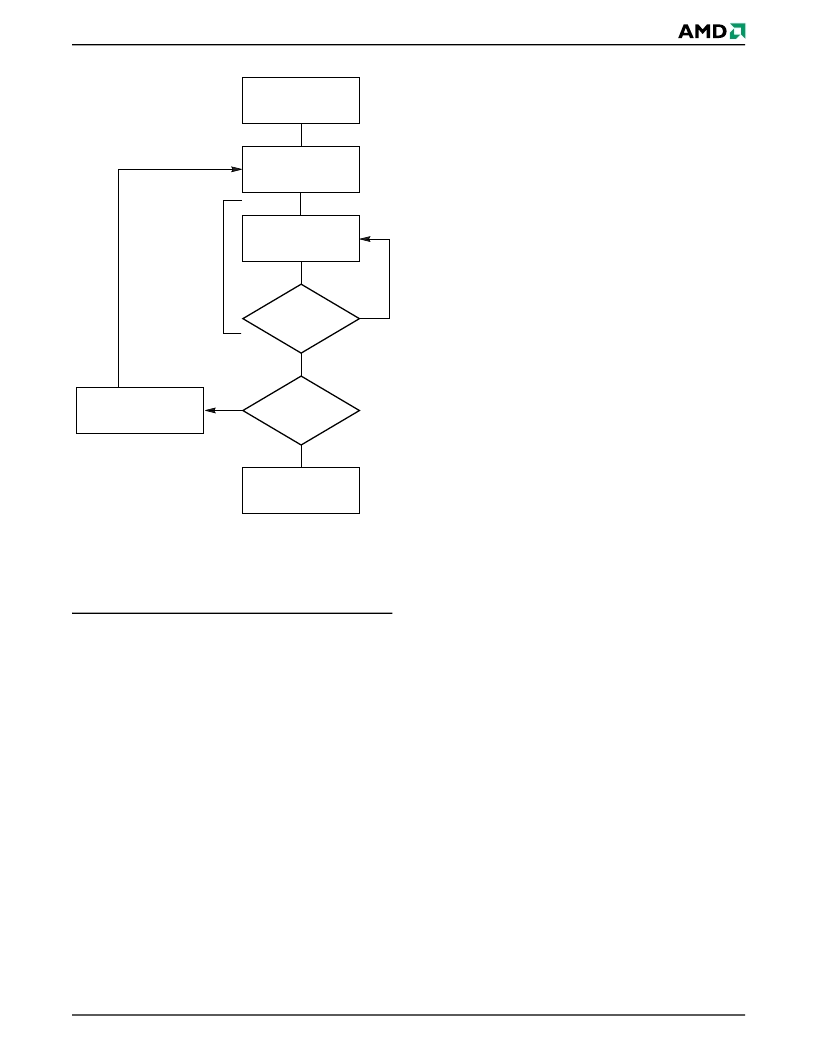
START
Write Program
Command Sequence
Data Poll
from System
Verify Data
No
Yes
Last Address
No
Yes
Programming
Completed
Increment Address
Embedded
Program
algorithm
in progress
相关PDF资料 |
PDF描述 |
|---|---|
| AM29F010B70PI | 1 Megabit (128 K x 8-bit) CMOS 5.0 Volt-only, Uniform Sector Flash Memory |
| AM29F010B70EC | LCD Module; Leaded Process Compatible:Yes RoHS Compliant: Yes |
| AM29F010B70EE | Segmented Alphanumeric LED; Display Technology:LED; No. of Digits/Alpha:1; Body Material:GaP; LED Color:Green; Leaded Process Compatible:Yes; Luminous Intensity:2.8mcd RoHS Compliant: Yes |
| AM29F010B70EI | Segmented Alphanumeric LED; Display Technology:LED; No. of Digits/Alpha:1; Body Material:GaAsP; LED Color:Red; Leaded Process Compatible:Yes; Luminous Intensity:3.3mcd RoHS Compliant: Yes |
| AM29F010B70FC | Segmented Alphanumeric LED; Display Technology:LED; No. of Digits/Alpha:1; Body Material:GaAsP; LED Color:Red; Leaded Process Compatible:Yes; Luminous Intensity:3.3mcd RoHS Compliant: Yes |
相关代理商/技术参数 |
参数描述 |
|---|---|
| AM29F010B-70PF | 制造商:Spansion 功能描述:Flash Memory IC |
| AM29F010B-90DPC 1 | 制造商:Spansion 功能描述:FLASH PARALLEL 5V 1MBIT 128KX8 90NS DIE - Gel-pak, waffle pack, wafer, diced wafer on film |
| AM29F010B-90ED | 制造商:Spansion 功能描述:IC FLASH 1MB SMD 29F010 TSOP32 |
| AM29F010B-90JC | 制造商:Analog Devices 功能描述:*IC AM29F010B-90JC |
| AM29F010B-90JD | 制造商:Spansion 功能描述:1M (128KX8) 5V UNIFORM SECTOR 制造商:Spansion 功能描述:FLASH 5V 1MB SMD 29F010 PLCC32 |
发布紧急采购,3分钟左右您将得到回复。