- 您现在的位置:买卖IC网 > PDF目录295065 > AM29F040B-150PEB (ADVANCED MICRO DEVICES INC) 4 Megabit (512 K x 8-Bit) CMOS 5.0 Volt-only, Uniform Sector Flash Memory PDF资料下载
参数资料
| 型号: | AM29F040B-150PEB |
| 厂商: | ADVANCED MICRO DEVICES INC |
| 元件分类: | PROM |
| 英文描述: | 4 Megabit (512 K x 8-Bit) CMOS 5.0 Volt-only, Uniform Sector Flash Memory |
| 中文描述: | 512K X 8 FLASH 5V PROM, 150 ns, PDIP32 |
| 封装: | PLASTIC, DIP-32 |
| 文件页数: | 27/30页 |
| 文件大小: | 417K |
| 代理商: | AM29F040B-150PEB |
第1页第2页第3页第4页第5页第6页第7页第8页第9页第10页第11页第12页第13页第14页第15页第16页第17页第18页第19页第20页第21页第22页第23页第24页第25页第26页当前第27页第28页第29页第30页
6
Am29F040B
DEVICE BUS OPERATIONS
This section describes the requirements and use of the
device bus operations, which are initiated through the
internal command register. The command register itself
does not occupy any addressable memory location.
The register is composed of latches that store the com-
mands, along with the address and data information
needed to execute the command. The contents of the
register serve as inputs to the internal state machine.
The state machine outputs dictate the function of the
device. The appropriate device bus operations table
lists the inputs and control levels required, and the re-
sulting output. The following subsections describe
each of these operations in further detail.
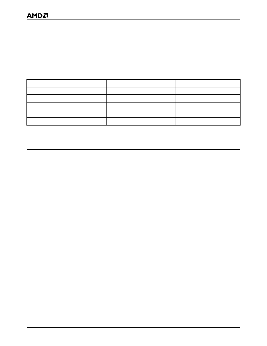
Table 1.
Am29F040B Device Bus Operations
Legend:
L = Logic Low = VIL, H = Logic High = VIH, VID = 12.0 ± 0.5 V, X = Don’t Care, DIN = Data In, DOUT = Data Out, AIN = Address In
Note: See the “Sector Protection/Unprotection” section. for more information.
Requirements for Reading Array Data
To read array data from the outputs, the system must
drive the CE# and OE# pins to VIL. CE# is the power
control and selects the device. OE# is the output con-
trol and gates array data to the output pins. WE#
should remain at VIH.
The internal state machine is set for reading array data
upon device power-up, or after a hardware reset. This
ensures that no spurious alteration of the memory con-
tent occurs during the power transition. No command is
necessary in this mode to obtain array data. Standard
microprocessor read cycles that assert valid addresses
on the device address inputs produce valid data on the
device data outputs. The device remains enabled for
read access until the command register contents are
altered.
See “Reading Array Data” for more information. Refer
to the AC Read Operations table for timing specifica-
tions and to the Read Operations Timings diagram for
the timing waveforms. ICC1 in the DC Characteristics
table represents the active current specification for
reading array data.
Writing Commands/Command Sequences
To write a command or command sequence (which in-
cludes programming data to the device and erasing
sectors of memory), the system must drive WE# and
CE# to VIL, and OE# to VIH.
An erase operation can erase one sector, multiple sec-
tors, or the entire device. The Sector Address Tables
indicate the address space that each sector occupies.
A “sector address” consists of the address bits required
to uniquely select a sector. See the “Command Defini-
tions” section for details on erasing a sector or the
e ntire chip, or suspendin g/resu ming the erase
operation.
After the system writes the autoselect command se-
quence, the device enters the autoselect mode. The
system can then read autoselect codes from the inter-
nal register (which is separate from the memory array)
on DQ7–DQ0. Standard read cycle timings apply in this
mode. Refer to the “Autoselect Mode” and “Autoselect
Command Sequence” sections for more information.
ICC2 in the DC Characteristics table represents the ac-
tive current specification for the write mode. The “AC
Characteristics” section contains timing specification
tables and timing diagrams for write operations.
Program and Erase Operation Status
During an erase or program operation, the system may
check the status of the operation by reading the status
bits on DQ7–DQ0. Standard read cycle timings and ICC
read specifications apply. Refer to “Write Operation
Status” for more information, and to each AC Charac-
teristics section for timing diagrams.
Standby Mode
When the system is not reading or writing to the device,
it can place the device in the standby mode. In this
mode, current consumption is greatly reduced, and the
Operation
CE#
OE#
WE#
A0–A20
DQ0–DQ7
Read
L
H
AIN
DOUT
Write
L
H
L
AIN
DIN
CMOS Standby
VCC ± 0.5 V
X
High-Z
TTL Standby
H
X
High-Z
Output Disable
L
H
X
High-Z
相关PDF资料 |
PDF描述 |
|---|---|
| AM29F040B-70EEB | 4 Megabit (512 K x 8-Bit) CMOS 5.0 Volt-only, Uniform Sector Flash Memory |
| AM29F040B-70FCB | 4 Megabit (512 K x 8-Bit) CMOS 5.0 Volt-only, Uniform Sector Flash Memory |
| AM29F040B-70FEB | 4 Megabit (512 K x 8-Bit) CMOS 5.0 Volt-only, Uniform Sector Flash Memory |
| AM29F040B-70FIB | 4 Megabit (512 K x 8-Bit) CMOS 5.0 Volt-only, Uniform Sector Flash Memory |
| AM29F040B-70JCB | 4 Megabit (512 K x 8-Bit) CMOS 5.0 Volt-only, Uniform Sector Flash Memory |
相关代理商/技术参数 |
参数描述 |
|---|---|
| AM29F040B-55EC | 制造商:Advanced Micro Devices 功能描述:NOR Flash, 512K x 8, 32 Pin, Plastic, TSSOP |
| AM29F040B-55ED | 制造商:Spansion 功能描述:IC FLASH 4MB SMD 29F040 TSOP32 |
| AM29F040B-55EE | 制造商:Spansion 功能描述:NOR Flash Parallel 5V 4Mbit 512K x 8bit 55ns 32-Pin TSOP |
| AM29F040B-55EF | 功能描述:闪存 4M (512Kx8) 55ns 5v Parallel NOR 闪存 RoHS:否 制造商:ON Semiconductor 数据总线宽度:1 bit 存储类型:Flash 存储容量:2 MB 结构:256 K x 8 定时类型: 接口类型:SPI 访问时间: 电源电压-最大:3.6 V 电源电压-最小:2.3 V 最大工作电流:15 mA 工作温度:- 40 C to + 85 C 安装风格:SMD/SMT 封装 / 箱体: 封装:Reel |
| AM29F040B-55EI | 制造商:Spansion 功能描述:NOR Flash Parallel 5V 4Mbit 512K x 8bit 55ns 32-Pin TSOP |
发布紧急采购,3分钟左右您将得到回复。