- 您现在的位置:买卖IC网 > PDF目录166213 > AM29F200BB-120ED (SPANSION LLC) Flash Memory IC; Leaded Process Compatible:Yes; Memory Size:2Mbit; Package/Case:48-TSOP; Peak Reflow Compatible (260 C):Yes; Supply Voltage Max:5V; Access Time, Tacc:120ns; Series:AM29 RoHS Compliant: Yes PDF资料下载
参数资料
| 型号: | AM29F200BB-120ED |
| 厂商: | SPANSION LLC |
| 元件分类: | PROM |
| 英文描述: | Flash Memory IC; Leaded Process Compatible:Yes; Memory Size:2Mbit; Package/Case:48-TSOP; Peak Reflow Compatible (260 C):Yes; Supply Voltage Max:5V; Access Time, Tacc:120ns; Series:AM29 RoHS Compliant: Yes |
| 中文描述: | 128K X 16 FLASH 5V PROM, 120 ns, PDSO48 |
| 封装: | LEAD FREE, MO-142DD, TSOP-48 |
| 文件页数: | 14/41页 |
| 文件大小: | 818K |
| 代理商: | AM29F200BB-120ED |
第1页第2页第3页第4页第5页第6页第7页第8页第9页第10页第11页第12页第13页当前第14页第15页第16页第17页第18页第19页第20页第21页第22页第23页第24页第25页第26页第27页第28页第29页第30页第31页第32页第33页第34页第35页第36页第37页第38页第39页第40页第41页
March 3, 2009 21526D5
Am29F200B
19
D A TA
SH EE T
the system must write the reset command to return to
reading array data.
The remaining scenario is that the system initially
determines that the toggle bit is toggling and DQ5 has
not gone high. The system may continue to monitor the
toggle bit and DQ5 through successive read cycles,
determining the status as described in the previous
paragraph. Alternatively, it may choose to perform
other system tasks. In this case, the system must start
at the beginning of the algorithm when it returns to
determine the status of the operation (top of Figure 5).
DQ5: Exceeded Timing Limits
DQ5 indicates whether the program or erase time has
exceeded a specified internal pulse count limit. Under
these conditions DQ5 produces a “1.” This is a failure
condition that indicates the program or erase cycle was
not successfully completed.
The DQ5 failure condition may appear if the system
tries to program a “1” to a location that is previously pro-
grammed to “0.” Only an erase operation can change
a “0” back to a “1.” Under this condition, the device
halts the operation, and when the operation has
exceeded the timing limits, DQ5 produces a “1.”
Under both these conditions, the system must issue the
reset command to return the device to reading array
data.
DQ3: Sector Erase Timer
After writing a sector erase command sequence, the
system may read DQ3 to determine whether or not an
erase operation has begun. (The sector erase timer
does not apply to the chip erase command.) If addi-
tional sectors are selected for erasure, the entire time-
out also applies after each additional sector erase com-
mand. When the time-out is complete, DQ3 switches
from “0” to “1.” The system may ignore DQ3 if the
system can guarantee that the time between additional
sector erase commands will always be less than 50
μs.
See also the “Sector Erase Command Sequence”
section.
After the sector erase command sequence is written,
the system should read the status on DQ7 (Data#
Polling) or DQ6 (Toggle Bit I) to ensure the device has
accepted the command sequence, and then read DQ3.
If DQ3 is “1”, the internally controlled erase cycle has
begun; all further commands (other than Erase Sus-
pend) are ignored until the erase operation is complete.
If DQ3 is “0”, the device will accept additional sector
erase commands. To ensure the command has been
accepted, the system software should check the status
of DQ3 prior to and following each subsequent sector
erase command. If DQ3 is high on the second status
check, the last command might not have been
accepted. Table 6 shows the outputs for DQ3.
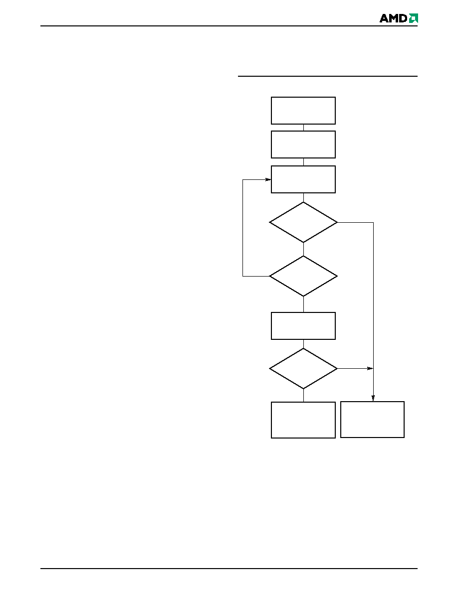
START
No
Yes
DQ5 = 1?
No
Yes
Toggle Bit
= Toggle?
No
Program/Erase
Operation Not
Complete, Write
Reset Command
Program/Erase
Operation Complete
Read DQ7–DQ0
Toggle Bit
= Toggle?
Read DQ7–DQ0
Twice
Read DQ7–DQ0
Notes:
1. Read toggle bit twice to determine whether or not it is
toggling. See text.
2. Recheck toggle bit because it may stop toggling as DQ5
changes to “1”. See text.
Figure 5.
Toggle Bit Algorithm
(Notes
相关PDF资料 |
PDF描述 |
|---|---|
| AM29F200BB-120EF | Flash Memory IC; Leaded Process Compatible:Yes; Memory Size:2Mbit; Package/Case:48-TSOP; Peak Reflow Compatible (260 C):Yes; Supply Voltage Max:5V; Access Time, Tacc:120ns; Series:AM29 RoHS Compliant: Yes |
| AM29F200BB-120SD | Flash Memory IC; Leaded Process Compatible:Yes; Memory Size:2Mbit; Package/Case:44-SOIC; Peak Reflow Compatible (260 C):Yes; Supply Voltage Max:5V; Access Time, Tacc:120ns; Series:AM29 RoHS Compliant: Yes |
| AM29F200BB-70EC | Flash Memory IC; Access Time, Tacc:70ns; Package/Case:48-TSOP; Leaded Process Compatible:No; Memory Configuration:256K x 8; Peak Reflow Compatible (260 C):No; Supply Voltage Max:5.5V; Mounting Type:Surface Mount RoHS Compliant: No |
| AM29F200BB-70ED | Flash Memory IC; Memory Size:2Mbit; Memory Configuration:256K x 8; Package/Case:48-TSOP; Leaded Process Compatible:Yes; Peak Reflow Compatible (260 C):Yes; Supply Voltage Max:5V; Access Time, Tacc:70ns; Mounting Type:Surface Mount RoHS Compliant: Yes |
| AM29F200BB-70EF | Flash Memory IC; Leaded Process Compatible:Yes; Memory Size:2Mbit; Package/Case:48-TSOP; Peak Reflow Compatible (260 C):Yes; Supply Voltage Max:5V; Access Time, Tacc:70ns; Series:AM29 RoHS Compliant: Yes |
相关代理商/技术参数 |
参数描述 |
|---|---|
| AM29F200BB-120SI | 制造商:Spansion 功能描述:NOR Flash Parallel 5V 2Mbit 256K/128K x 8bit/16bit 120ns 44-Pin SOIC |
| AM29F200BB-120SI\T | 制造商:Spansion 功能描述:Flash Mem Parallel 5V 2M-Bit 256K x 8/128K x 16 120ns 44-Pin SOIC T/R |
| AM29F200BB-45SI | 制造商:Advanced Micro Devices 功能描述: |
| AM29F200BB-55EF | 功能描述:闪存 2M (256KX8/128KX16) Parallel NOR Fl 5V RoHS:否 制造商:ON Semiconductor 数据总线宽度:1 bit 存储类型:Flash 存储容量:2 MB 结构:256 K x 8 定时类型: 接口类型:SPI 访问时间: 电源电压-最大:3.6 V 电源电压-最小:2.3 V 最大工作电流:15 mA 工作温度:- 40 C to + 85 C 安装风格:SMD/SMT 封装 / 箱体: 封装:Reel |
| AM29F200BB-55EF\T | 制造商:Spansion 功能描述:NOR Flash Parallel 5V 2Mbit 256K/128K x 8bit/16bit 55ns 48-Pin TSOP T/R |
发布紧急采购,3分钟左右您将得到回复。