- 您现在的位置:买卖IC网 > PDF目录366487 > AM29LV160DB-70SC (Advanced Micro Devices, Inc.) 16 Megabit (2 M x 8-Bit/1 M x 16-Bit) CMOS 3.0 Volt-only Boot Sector Flash Memory PDF资料下载
参数资料
| 型号: | AM29LV160DB-70SC |
| 厂商: | Advanced Micro Devices, Inc. |
| 元件分类: | FLASH |
| 英文描述: | 16 Megabit (2 M x 8-Bit/1 M x 16-Bit) CMOS 3.0 Volt-only Boot Sector Flash Memory |
| 中文描述: | 16Mb(2M×8位/1Mx16位), 3V, CMOS引导扇区闪存 |
| 文件页数: | 23/52页 |
| 文件大小: | 844K |
| 代理商: | AM29LV160DB-70SC |
第1页第2页第3页第4页第5页第6页第7页第8页第9页第10页第11页第12页第13页第14页第15页第16页第17页第18页第19页第20页第21页第22页当前第23页第24页第25页第26页第27页第28页第29页第30页第31页第32页第33页第34页第35页第36页第37页第38页第39页第40页第41页第42页第43页第44页第45页第46页第47页第48页第49页第50页第51页第52页
22358B7
May 5, 2006
Am29LV160D
21
D A T A S H E E T
Any commands written to the device during the Em-
bedded Program Algorithm are ignored. Note that a
hardware reset
immediately terminates the program-
ming operation. The Byte Program command
sequence should be reinitiated once the device has
reset to reading array data, to ensure data integrity.
Programming is allowed in any sequence and across
sector boundaries.
A bit cannot be programmed
from a “0” back to a “1”.
Attempting to do so may
halt the operation and set DQ5 to “1,” or cause the
Data# Polling algorithm to indicate the operation was
successful. However, a succeeding read will show that
the data is still “0”. Only erase operations can convert
a “0” to a “1”.
Unlock Bypass Command Sequence
The unlock bypass feature allows the system to pro-
gram bytes or words to the device faster than using the
standard program command sequence. The unlock
bypass command sequence is initiated by first writing
two unlock cycles. This is followed by a third write
cycle containing the unlock bypass command, 20h.
The device then enters the unlock bypass mode. A
two-cycle unlock bypass program command sequence
is all that is required to program in this mode. The first
cycle in this sequence contains the unlock bypass pro-
gram command, A0h; the second cycle contains the
program address and data. Additional data is pro-
grammed in the same manner. This mode dispenses
with the initial two unlock cycles required in the stan-
dard program command sequence, resulting in faster
total programming time. Table 9 shows the require-
ments for the command sequence.
During the unlock bypass mode, only the Unlock By-
pass Program and Unlock Bypass Reset commands
are valid. To exit the unlock bypass mode, the system
must issue the two-cycle unlock bypass reset com-
mand sequence. The first cycle must contain the data
Note:
See Table 9 for program command sequence.
90h; the second cycle the data 00h. Addresses are
don’t care for both cycles. The device then returns to
reading array data.
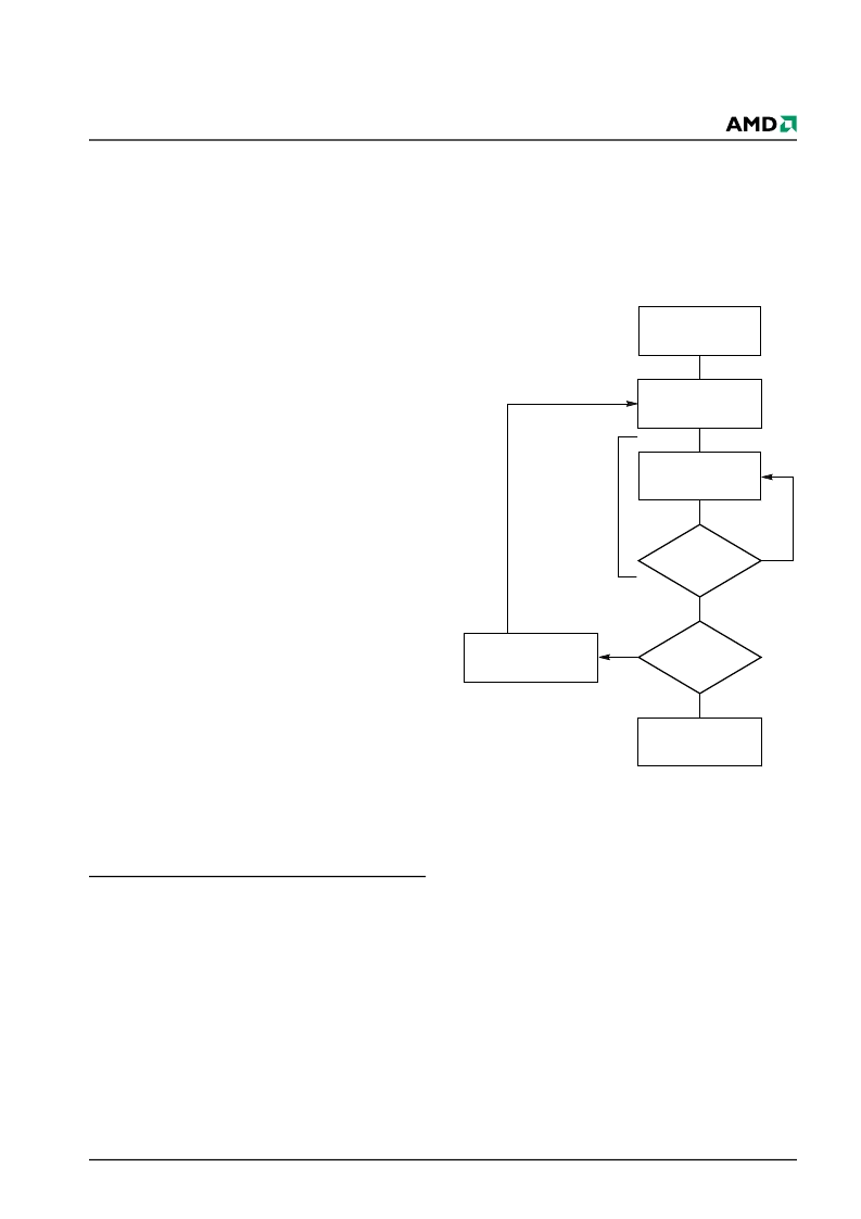
Figure 3 illustrates the algorithm for the program oper-
ation. See the Erase/Program Operations table in “AC
Characteristics” for parameters, and to Figure 17 for
timing diagrams.
Figure 3. Program Operation
Chip Erase Command Sequence
Chip erase is a six bus cycle operation. The chip erase
command sequence is initiated by writing two unlock
cycles, followed by a set-up command. Two additional
unlock write cycles are then followed by the chip erase
command, which in turn invokes the Embedded Erase
algorithm. The device does
not
require the system to
preprogram prior to erase. The Embedded Erase algo-
rithm automatically preprograms and verifies the entire
memory for an all zero data pattern prior to electrical
erase. The system is not required to provide any con-
trols or timings during these operations. Table 9 shows
the address and data requirements for the chip erase
command sequence.
Any commands written to the chip during the Embed-
ded Erase algorithm are ignored. Note that a
hardware reset
during the chip erase operation im-
mediately terminates the operation. The Chip Erase
command sequence should be reinitiated once the de-
vice has returned to reading array data, to ensure data
integrity.
The system can determine the status of the erase op-
eration by using DQ7, DQ6, DQ2, or RY/BY#. See
“Write Operation Status” for information on these sta-
tus bits. When the Embedded Erase algorithm is
complete, the device returns to reading array data and
addresses are no longer latched.
START
Write Program
Command Sequence
Data Poll
from System
Verify Data
No
Yes
Last Address
No
Yes
Programming
Completed
Increment Address
Embedded
Program
algorithm
in progress
相关PDF资料 |
PDF描述 |
|---|---|
| AM29LV160DB-70SD | 16 Megabit (2 M x 8-Bit/1 M x 16-Bit) CMOS 3.0 Volt-only Boot Sector Flash Memory |
| AM29LV160DB-70SF | 16 Megabit (2 M x 8-Bit/1 M x 16-Bit) CMOS 3.0 Volt-only Boot Sector Flash Memory |
| AM29LV160DB-70SI | 16 Megabit (2 M x 8-Bit/1 M x 16-Bit) CMOS 3.0 Volt-only Boot Sector Flash Memory |
| AM29LV160DB-70WCD | 16 Megabit (2 M x 8-Bit/1 M x 16-Bit) CMOS 3.0 Volt-only Boot Sector Flash Memory |
| AM29LV160DB-70WCF | 16 Megabit (2 M x 8-Bit/1 M x 16-Bit) CMOS 3.0 Volt-only Boot Sector Flash Memory |
相关代理商/技术参数 |
参数描述 |
|---|---|
| AM29LV160DB-70SI | 制造商: 功能描述: 制造商:undefined 功能描述: |
| AM29LV160DB-90EC | 制造商:Advanced Micro Devices 功能描述: |
| AM29LV160DB90EI | 制造商:AMD 功能描述:NEW 制造商:SOCO 功能描述: 制造商:Spansion 功能描述: |
| AM29LV160DB-90EI | 制造商:Advanced Micro Devices 功能描述: |
| AM29LV160DB-90EI\\T | 制造商:Advanced Micro Devices 功能描述: |
发布紧急采购,3分钟左右您将得到回复。