- 您现在的位置:买卖IC网 > PDF目录362306 > AMC78L05DMF (Electronic Theatre Controls, Inc.) 100mA / 3-TERMINAL 5V REGULATOR PDF资料下载
参数资料
| 型号: | AMC78L05DMF |
| 厂商: | Electronic Theatre Controls, Inc. |
| 英文描述: | 100mA / 3-TERMINAL 5V REGULATOR |
| 中文描述: | 百毫安/三端5V稳压器 |
| 文件页数: | 14/28页 |
| 文件大小: | 468K |
| 代理商: | AMC78L05DMF |
第1页第2页第3页第4页第5页第6页第7页第8页第9页第10页第11页第12页第13页当前第14页第15页第16页第17页第18页第19页第20页第21页第22页第23页第24页第25页第26页第27页第28页
AMC7820
SBAS231B
www.ti.com
14
OVERVIEW
The AMC7820 is an analog monitoring and control circuit for
control of laser diodes and TEC coolers in DWDM applica-
tions. A register-based architecture eases integration with
DSP-based (or microprocessor-based) systems through a
standard SPI bus. All peripheral functions are controlled
through the registers and onboard state machines.
The AMC7820 consists of the following blocks (refer to the
block diagram of Figure 2):
8-Channel, 12-Bit ADC
Three 12-Bit DACs
Nine Operational Amplifiers
+2.5V Reference
TEC Soft Start Controller
Communication to the AMC7820 is via a standard SPI serial
interface. This interface requires that
SS
, the Slave Select
signal, be driven LOW to communicate with the AMC7820.
The data is then shifted into and out of the AMC7820 under
control of the host DSP or microprocessor, which also
provides the serial data clock.
Control of the AMC7820 and its functions is accomplished by
writing to different registers in the AMC7820. A simple com-
mand protocol is used to address the 16-bit registers. Regis-
ters control the operation of the ADC, DACs, and device
configuration. The results of measurements made are placed
in the memory map and can be read by the host at any time.
All pins have ESD protection circuitry as the first active
element on the chip. All input and output pins have protection
diodes connected to supply and ground that remain reverse
biased under normal operation. If the input voltages exceed
the absolute maximum voltage range, it is necessary to add
resistance in series with the input to limit the current to 10mA
or less.
ADC
The analog inputs are provided via a multiplexer to the
Successive Approximation Register (SAR) ADC. The ADC
architecture is based on capacitive redistribution architecture
that inherently includes a sample-and-hold function.
The multiplexer provides eight analog input channels to the
ADC. Channels 0, 1, 6, and 7 are buffered by amplifiers
OPA3, OPA4, OPA5, and OPA6, respectively. Channels 2,
3, 4, and 5 connect directly to external pins. The multiplexer
connects each analog input to the ADC sequentially. Analog
current into the device must charge the internal sample-
and-hold capacitor during the sampling period. When the
converter is in Hold mode, and the sampling capacitor has
been fully charged, the input impedance of the analog input
is greater than 1G
.
The on resistance of each multiplexer switch is typically
150
. In order to charge the internal sample-and-hold ca-
pacitor completely during the acquisition time, the source
impedance of the analog input should be no more than 1k
.
The ADC runs continuously upon start-up, scanning through
each channel. The results of conversions made are stored in
the appropriate ADC registers.
Since the input range of the ADC is 2
V
REF
, codes near FFF
will be missing if the output range of the signal source driving
an ADC input channel is limited to less than 2
V
REF
. This is
the case for channels 0, 1, 6, and 7 which are driven from
internal op amps which have an output range limit of AV
DD
.
If all codes including FFF are required, the value of the
reference voltage must be reduced or the value of AV
DD
must
be increased.
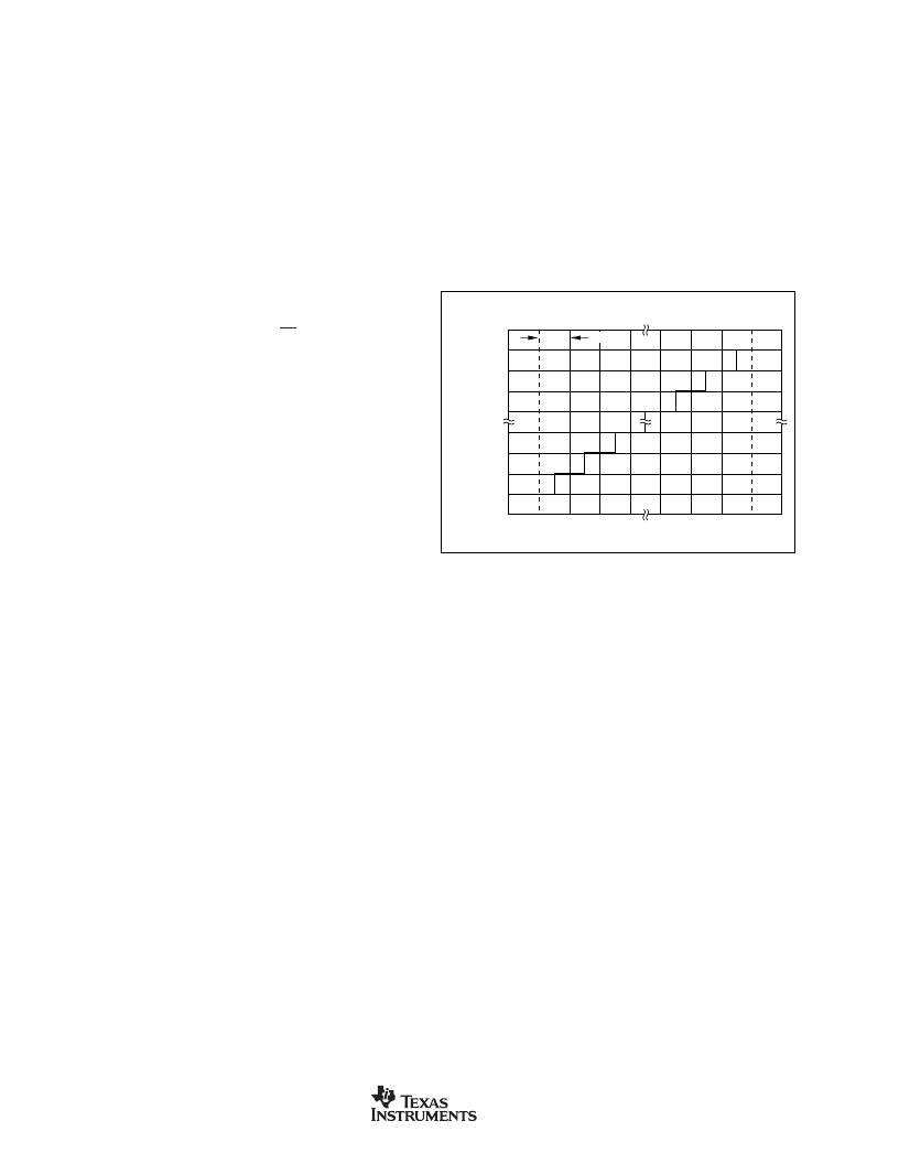
Data Format
The AMC7820 output data is in Straight Binary format, as
shown in Figure 1. This figure shows the ideal output code for
the given input voltage and does not include the effects of
offset, gain, or noise.
DACS
The three 12-bit DACs of the AMC7820 use a resistor-string
architecture with switchable taps that are buffered by an
operational amplifier (see DAC0 in Figure 4). Each op amp
buffer can be configured for a gain of +1 or +2, which sets the
output range to 0V to +2.5V or 0V to +5.0V, respectively. This
architecture is inherently monotonic, a critical requirement for
any system requiring
“
smooth
”
setpoint control.
The op amp buffer has a rail-to-rail output stage that has
limitations on sinking or sourcing current when the output
voltage is near AGND or AV
DD
, respectively (see the typical
characteristics). For example, if a DAC (Gain = +1) is set to
code 010
H
(+10mV) and is required to sink 1mA of current,
the DAC output voltage will be approximately 250mV instead
of the desired value of +10mV.
This problem is solved by restricting the DAC output voltage
to values greater than +250mV or by reducing the required
sink current. This restriction does not apply for the case of
sourcing current for gain set at +1. When the gain is set at +2,
there is a limitation on sourcing current with the output
voltage near the positive supply rail.
The slope of the DAC output voltage curve for sinking or
sourcing current is due to an increase in the inherent closed-
loop output impedance of the operational amplifier buffer, when
operating near a supply rail.
Refer to the typical characteristic
curves.
FIGURE 1. Ideal Input Voltage and Output Codes.
O
0V
FS = Full-Scale Voltage = 2V
REF
1LSB = 2V
REF
/4096
FS
–
1LSB
11...111
11...110
11...101
00...010
00...001
00...000
1LSB
Input Voltage (V)
相关PDF资料 |
PDF描述 |
|---|---|
| AMC78L05LP | 100mA / 3-TERMINAL 5V REGULATOR |
| AMC78L05LPF | 100mA / 3-TERMINAL 5V REGULATOR |
| AMC78L05PK | 100mA / 3-TERMINAL 5V REGULATOR |
| AMC78L05PKF | 100mA / 3-TERMINAL 5V REGULATOR |
| AMCK-67142V-35R | 2K X 8 CMOS DUAL PORT RAM |
相关代理商/技术参数 |
参数描述 |
|---|---|
| AMC78L05LP | 制造商:ADDTEK 制造商全称:ADDTEK 功能描述:100mA / 3-TERMINAL 5V REGULATOR |
| AMC78L05LPF | 制造商:ADDTEK 制造商全称:ADDTEK 功能描述:100mA / 3-TERMINAL 5V REGULATOR |
| AMC78L05PK | 制造商:ADDTEK 制造商全称:ADDTEK 功能描述:100mA / 3-TERMINAL 5V REGULATOR |
| AMC78L05PKF | 制造商:ADDTEK 制造商全称:ADDTEK 功能描述:100mA / 3-TERMINAL 5V REGULATOR |
| AMC78N-V00 | 制造商:Panasonic Industrial Company 功能描述:HOLDER |
发布紧急采购,3分钟左右您将得到回复。