参数资料
| 型号: | AMP04EPZ |
| 厂商: | Analog Devices Inc |
| 文件页数: | 14/16页 |
| 文件大小: | 0K |
| 描述: | IC AMP INST PREC 30MA LP 8DIP |
| 标准包装: | 50 |
| 放大器类型: | 仪表 |
| 电路数: | 1 |
| -3db带宽: | 700kHz |
| 电流 - 输入偏压: | 22nA |
| 电压 - 输入偏移: | 30µV |
| 电流 - 电源: | 750µA |
| 电流 - 输出 / 通道: | 30mA |
| 电压 - 电源,单路/双路(±): | 5 V ~ 30 V,±2.5 V ~ 15 V |
| 工作温度: | -40°C ~ 85°C |
| 安装类型: | 通孔 |
| 封装/外壳: | 8-DIP(0.300",7.62mm) |
| 供应商设备封装: | 8-PDIP |
| 包装: | 管件 |
| 产品目录页面: | 771 (CN2011-ZH PDF) |
AMP04
REV. B
–7–
Programming the Gain
The gain of the AMP04 is programmed by the user by selecting
a single external resistor—RGAIN:
Gain = 100 k
/RGAIN
The output voltage is then defined as the differential input
voltage times the gain.
VOUT = (VIN+ – VIN–)
× Gain
In single supply systems, offsetting the ground is often desired
for several reasons. Ground may be offset from zero to provide
a quieter signal reference point, or to offset “zero” to allow a
unipolar signal range to represent both positive and negative
values.
In noisy environments such as those having digital switching,
switching power supplies or externally generated noise, ground
may not be the ideal place to reference a signal in a high accu-
racy system.
Often, real world signals such as temperature or pressure may
generate voltages that are represented by changes in polarity. In
a single supply system the signal input cannot be allowed to go
below ground, and therefore the signal must be offset to accom-
modate this change in polarity. On the AMP04, a reference
input pin is provided to allow offsetting of the input range.
The gain equation is more accurately represented by including
this reference input.
VOUT = (VIN+ – VIN–)
× Gain + VREF
Grounding
The most common problems encountered in high performance
analog instrumentation and data acquisition system designs are
found in the management of offset errors and ground noise.
Primarily, the designer must consider temperature differentials
and thermocouple effects due to dissimilar metals, IR volt-
age drops, and the effects of stray capacitance. The problem
is greatly compounded when high speed digital circuitry, such
as that accompanying data conversion components, is brought
into the proximity of the analog section. Considerable noise and
error contributions such as fast-moving logic signals that easily
propagate into sensitive analog lines, and the unavoidable noise
common to digital supply lines must all be dealt with if the accu-
racy of the carefully designed analog section is to be preserved.
Besides the temperature drift errors encountered in the ampli-
fier, thermal errors due to the supporting discrete components
should be evaluated. The use of high quality, low-TC compo-
nents where appropriate is encouraged. What is more important,
large thermal gradients can create not only unexpected changes
in component values, but also generate significant thermoelec-
tric voltages due to the interface between dissimilar metals such
as lead solder, copper wire, gold socket contacts, Kovar lead
frames, etc. Thermocouple voltages developed at these junctions
commonly exceed the TCVOS contribution of the AMP04.
Component layout that takes into account the power dissipation
at critical locations in the circuit and minimizes gradient effects
and differential common-mode voltages by taking advantage of
input symmetry will minimize many of these errors.
High accuracy circuitry can experience considerable error con-
tributions due to the coupling of stray voltages into sensitive
areas, including high impedance amplifier inputs which benefit
from such techniques as ground planes, guard rings, and shields.
Careful circuit layout, including good grounding and signal
routing practice to minimize stray coupling and ground loops is
recommended. Leakage currents can be minimized by using
high quality socket and circuit board materials, and by carefully
cleaning and coating complete board assemblies.
As mentioned above, the high speed transition noise found in
logic circuitry is the sworn enemy of the analog circuit designer.
Great care must be taken to maintain separation between them
to minimize coupling. A major path for these error voltages will
be found in the power supply lines. Low impedance, load related
variations and noise levels that are completely acceptable in the
high thresholds of the digital domain make the digital supply
unusable in nearly all high performance analog applications.
The user is encouraged to maintain separate power and ground
between the analog and digital systems wherever possible,
joining only at the supply itself if necessary, and to observe
careful grounding layout and bypass capacitor scheduling in
sensitive areas.
Input Shield Drivers
High impedance sources and long cable runs from remote trans-
ducers in noisy industrial environments commonly experience
significant amounts of noise coupled to the inputs. Both stray
capacitance errors and noise coupling from external sources can
be minimized by running the input signal through shielded
cable. The cable shield is often grounded at the analog input
common, however improved dynamic noise rejection and a
reduction in effective cable capacitance is achieved by driving
the shield with a buffer amplifier at a potential equal to the
voltage seen at the input. Driven shields are easily realized with
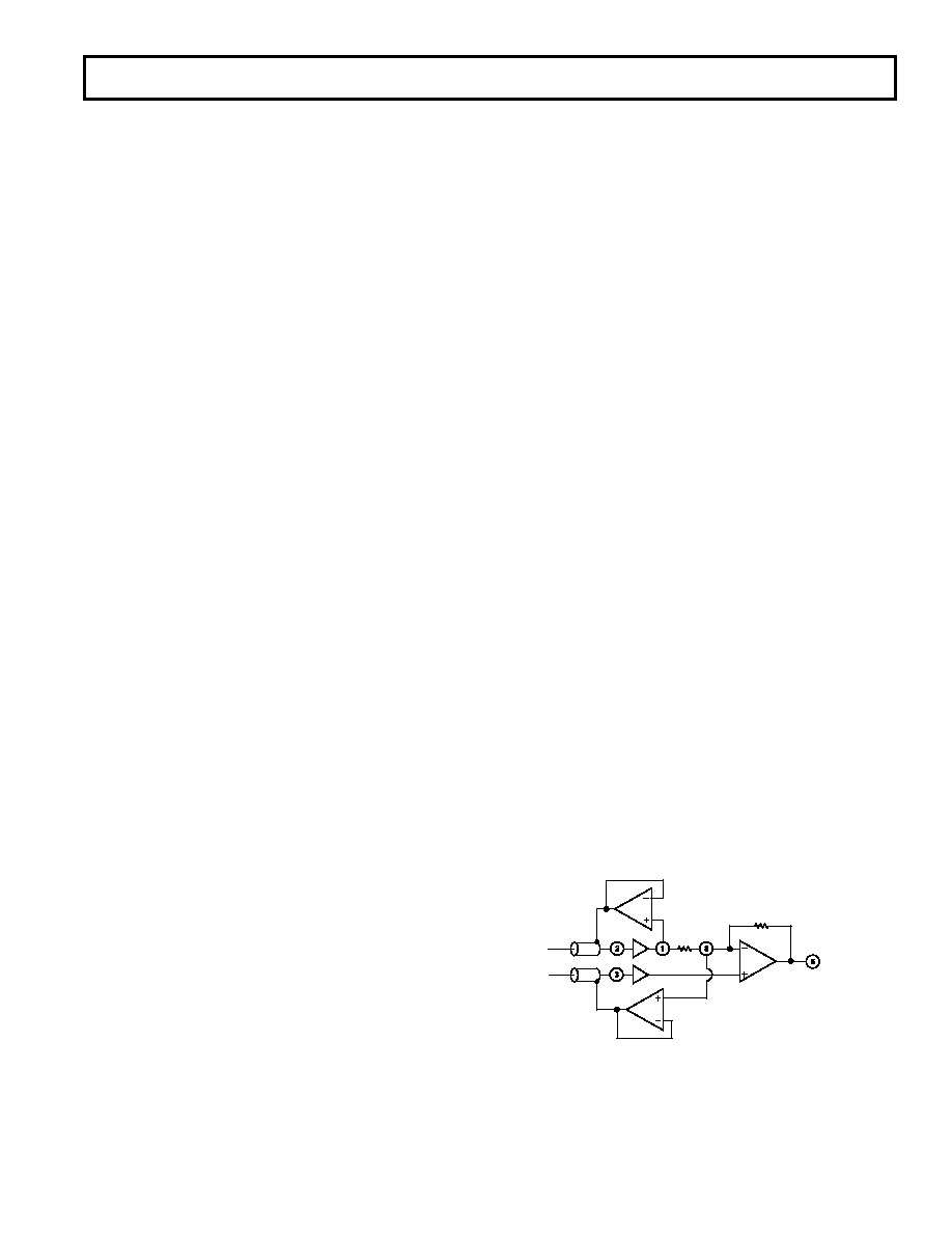
the AMP04. Examination of the simplified schematic shows that
the potentials at the gain set resistor pins of the AMP04 follow
the inputs precisely. As shown in Figure 5, shield drivers are
easily realized by buffering the potential at these pins by a dual,
single supply op amp such as the OP213. Alternatively, applica-
tions with single-ended sources or that use twisted-pair cable
could drive a single shield. To minimize error contributions due
to this additional circuitry, all components and wiring should
remain in proximity to the AMP04 and careful grounding and
bypassing techniques should be observed.
VOUT
1/2 OP213
Figure 5. Cable Shield Drivers
相关PDF资料 |
PDF描述 |
|---|---|
| 9-146282-0-28 | CONN HDR BRKWAY .100 28POS VERT |
| 4-103741-0-28 | CONN HEADR BRKWAY .100 28POS STR |
| OP297EZ | IC OPAMP GP 500KHZ DUAL 8CDIP |
| OP270EZ | IC OPAMP GP 5MHZ DUAL PREC 8CDIP |
| 929647-09-04-I | CONN HEADER .100 SNGL STR 4POS |
相关代理商/技术参数 |
参数描述 |
|---|---|
| AMP04EPZ | 制造商:Analog Devices 功能描述:Instrumentation Amplifier |
| AMP04ES | 功能描述:IC AMP INST PREC 30MA LP 8SOIC RoHS:否 类别:集成电路 (IC) >> Linear - Amplifiers - Instrumentation 系列:- 标准包装:2,500 系列:- 放大器类型:通用 电路数:1 输出类型:满摆幅 转换速率:0.11 V/µs 增益带宽积:350kHz -3db带宽:- 电流 - 输入偏压:4nA 电压 - 输入偏移:20µV 电流 - 电源:260µA 电流 - 输出 / 通道:20mA 电压 - 电源,单路/双路(±):2.7 V ~ 36 V,±1.35 V ~ 18 V 工作温度:-40°C ~ 85°C 安装类型:表面贴装 封装/外壳:8-SOIC(0.154",3.90mm 宽) 供应商设备封装:8-SO 包装:带卷 (TR) |
| AMP04ES-REEL7 | 制造商:Analog Devices 功能描述:SP Amp INSTR Amp Single ±15V/30V 8-Pin SOIC T/R |
| AMP04ESZ | 功能描述:IC AMP INST PREC 30MA LP 8SOIC RoHS:是 类别:集成电路 (IC) >> Linear - Amplifiers - Instrumentation 系列:- 标准包装:2,500 系列:- 放大器类型:通用 电路数:4 输出类型:- 转换速率:0.6 V/µs 增益带宽积:1MHz -3db带宽:- 电流 - 输入偏压:45nA 电压 - 输入偏移:2000µV 电流 - 电源:1.4mA 电流 - 输出 / 通道:40mA 电压 - 电源,单路/双路(±):3 V ~ 32 V,±1.5 V ~ 16 V 工作温度:0°C ~ 70°C 安装类型:表面贴装 封装/外壳:14-TSSOP(0.173",4.40mm 宽) 供应商设备封装:14-TSSOP 包装:带卷 (TR) 其它名称:LM324ADTBR2G-NDLM324ADTBR2GOSTR |
| AMP04ESZ | 制造商:Analog Devices 功能描述:IC, INSTRUMENT AMP, 700KHZ, 85DB, SOIC-8 |
发布紧急采购,3分钟左右您将得到回复。