参数资料
| 型号: | AMP04FSZ-RL |
| 厂商: | Analog Devices Inc |
| 文件页数: | 15/16页 |
| 文件大小: | 0K |
| 描述: | IC AMP INST PREC 30MA LP 8SOIC |
| 标准包装: | 2,500 |
| 放大器类型: | 仪表 |
| 电路数: | 1 |
| -3db带宽: | 700kHz |
| 电流 - 输入偏压: | 22nA |
| 电压 - 输入偏移: | 30µV |
| 电流 - 电源: | 750µA |
| 电流 - 输出 / 通道: | 30mA |
| 电压 - 电源,单路/双路(±): | 5 V ~ 30 V,±2.5 V ~ 15 V |
| 工作温度: | -40°C ~ 85°C |
| 安装类型: | 表面贴装 |
| 封装/外壳: | 8-SOIC(0.154",3.90mm 宽) |
| 供应商设备封装: | 8-SOIC |
| 包装: | 带卷 (TR) |
AMP04
REV. B
–8–
Compensating for Input and Output Errors
To achieve optimal performance, the user needs to take into
account a number of error sources found in instrumentation
amplifiers. These consist primarily of input and output offset
voltages and leakage currents.
The input and output offset voltages are independent from one
another, and must be considered separately. The input offset
component will of course be directly multiplied by the gain of
the amplifier, in contrast to the output offset voltage that is
independent of gain. Therefore, the output error is the domi-
nant factor at low gains, and the input error grows to become
the greater problem as gain is increased. The overall equation
for offset voltage error referred to the output (RTO) is:
VOS (RTO) = (VIOS
× G) + V
OOS
where VIOS is the input offset voltage and VOOS the output offset
voltage, and G is the programmed amplifier gain.
The change in these error voltages with temperature must also
be taken into account. The specification TCVOS, referred to the
output, is a combination of the input and output drift specifica-
tions. Again, the gain influences the input error but not the
output, and the equation is:
TCVOS (RTO) = (TCVIOS
× G) + TCVOOS
In some applications the user may wish to define the error con-
tribution as referred to the input, and treat it as an input error.
The relationship is:
TCVOS (RTI) = TCVIOS + (TCVOOS / G)
The bias and offset currents of the input transistors also have an
impact on the overall accuracy of the input signal. The input
leakage, or bias currents of both inputs will generate an addi-
tional offset voltage when flowing through the signal source
resistance. Changes in this error component due to variations
with signal voltage and temperature can be minimized if both
input source resistances are equal, reducing the error to a
common-mode voltage which can be rejected. The difference in
bias current between the inputs, the offset current, generates a
differential error voltage across the source resistance that should
be taken into account in the user’s design.
In applications utilizing floating sources such as thermocouples,
transformers, and some photo detectors, the user must take
care to provide some current path between the high imped-
ance inputs and analog ground. The input bias currents of
the AMP04, although extremely low, will charge the stray
capacitance found in nearby circuit traces, cables, etc., and
cause the input to drift erratically or to saturate unless given a
bleed path to the analog common. Again, the use of equal resis-
tance values will create a common input error voltage that is
rejected by the amplifier.
Reference Input
The VREF input is used to set the system ground. For dual sup-
ply operation it can be connected to ground to give zero volts
out with zero volts differential input. In single supply systems it
could be connected either to the negative supply or to a pseudo-
ground between the supplies. In any case, the REF input must
be driven with low impedance.
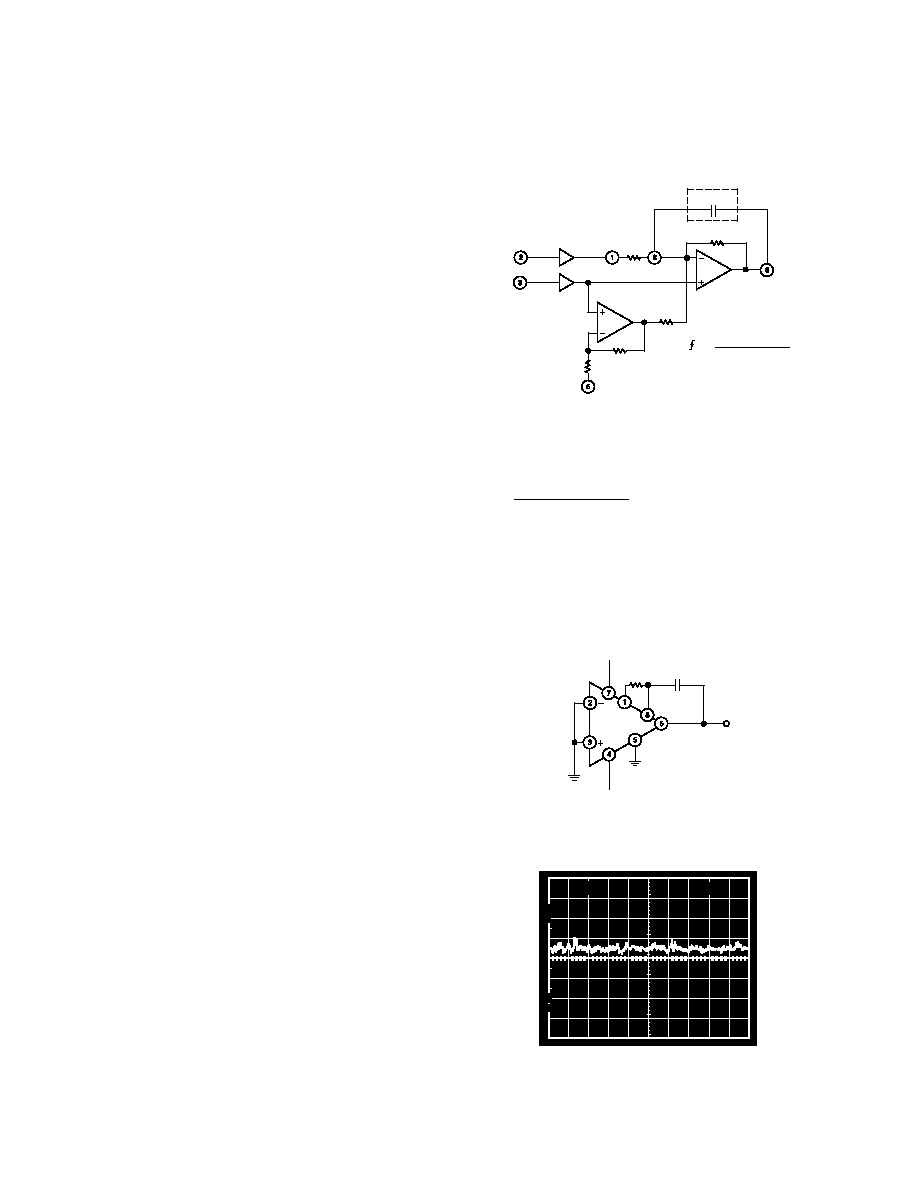
Noise Filtering
Unlike most previous instrumentation amplifiers, the output
stage’s inverting input (Pin 8) is accessible. By placing a capaci-
tor across the AMP04’s feedback path (Figure 6, Pins 6 and 8)
IN(–)
IN(+)
INPUT BUFFERS
REF
100k
LP =
1
2
(100k ) CEXT
11k
RGAIN
VOUT
100k
CEXT
Figure 6. Noise Band Limiting
a single-pole low-pass filter is produced. The cutoff frequency
(fLP) follows the relationship:
f
LP =
1
2
π (100 k) C
EXT
Filtering can be applied to reduce wide band noise. Figure 7a
shows a 10 Hz low-pass filter, gain of 1000 for the AMP04.
Figures 7b and 7c illustrate the effect of filtering on noise. The
photo in Figure 7b shows the output noise before filtering. By
adding a 0.15
F capacitor, the noise is reduced by about a
factor of 4 as shown in Figure 7c.
100k
+15V
–15V
0.15 F
Figure 7a. 10 Hz Low-Pass Filter
10
90
100
0%
5mV
10ms
Figure 7b. Unfiltered AMP04 Output
相关PDF资料 |
PDF描述 |
|---|---|
| SM6S30AHE3/2D | TVS 6W 30V 5% SMD DO-218AB |
| LTC1100CN8 | IC INSTRMNT AMP CHOP-STABL 8-DIP |
| SM6S28AHE3/2D | TVS 6W 28V 5% SMD DO-218AB |
| FWJ-500A | FUSE 500A 1000V UL |
| LT2078AIS8#TRPBF | IC OPAMP MICROPOWER DUAL 8-SOIC |
相关代理商/技术参数 |
参数描述 |
|---|---|
| AMP04GBC | 制造商:Analog Devices 功能描述:PRECISION SINGLE SUPPLY INSTRUMENTATION |
| AMP-05 | 制造商:未知厂家 制造商全称:未知厂家 功能描述:Operational Amplifier |
| AMP-0-5492458-1 | 制造商:TE Connectivity 功能描述:CONN FIBER ST PLUG SMPLX 125UM |
| AMP-0-5749769-1 | 制造商:TE Connectivity 功能描述:CONN D-SUB PLUG R/A 26POS 30GOLD |
| AMP05AX | 制造商:未知厂家 制造商全称:未知厂家 功能描述:Instrumentation Amp, Resistor-Programmable |
发布紧急采购,3分钟左右您将得到回复。