- 您现在的位置:买卖IC网 > PDF目录378403 > AN1025 (Microchip Technology Inc.) Converting A 5.0V Supply Rail To A Regulated 3.0V PDF资料下载
参数资料
| 型号: | AN1025 |
| 厂商: | Microchip Technology Inc. |
| 英文描述: | Converting A 5.0V Supply Rail To A Regulated 3.0V |
| 中文描述: | 5.0V电源转换阿铁至一个稳压3.0V |
| 文件页数: | 3/8页 |
| 文件大小: | 531K |
| 代理商: | AN1025 |
2006 Microchip Technology Inc.
DS01025A-page 3
AN1025
CHARGE PUMP
A charge pump is another regulator topology that can
be used to convert a 5.0V system rail voltage down to
a regulated 3.0V to be used by microcontrollers or
other logic. Charge pumps, also referred to as an
inductor-less DC-DC converter or a switched-capacitor
circuit, are just as easy to use as LDOs. Like an LDO,
a charge pump requires an input and output capacitor
and a feedback resistor divider network. However,
charge pumps require an additional charge storing
capacitor which is sometimes referred to as a fly
capacitor.
There are many different types of charge pumps. Some
of the more common types are: voltage inverting,
voltage doubling, regulated buck, regulated boost
and
regulated buck/boost. The regulated buck charge
pump is the only type that is discussed in this
application note. For information on the other types of
charge pumps, refer to the Microchip web site at
www.microchip.com.
Regulated Buck Charge Pump Operation
Microchip’s MCP1252/3 is a positive regulated charge
pump that, like most charge pumps, uses four
MOSFET switches to control the charge and discharge
of the fly capacitor and thereby regulates the output
voltage. However, unlike most charge pumps, the
MCP1252/3 allows for the source voltage to be lower or
higher that the output voltage by automatically
switching between buck/boost operation. For the
purpose of this application note, the Buck mode is the
only operating state that is discussed. Refer to the
MCP1252/3 Data Sheet (DS21752) for a full
description of the buck/boost operation.
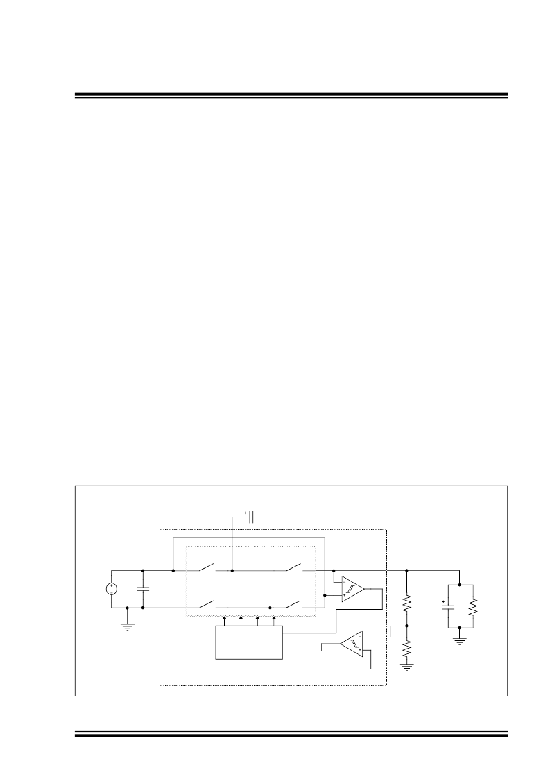
In Figure 3, it can be seen that the internal comparator
U1, determines which mode the MCP1252/3 operates
in. While in Buck mode, the positive input node is
greater than the negative input node, switch SW1 is
always closed, and SW2 is always open. When the
MCP1252/3 is not in Shutdown mode and a steady-
state condition has been reached, there are three
phases of operation. During the first phase, charge is
transferred from the input source to C
FLY
by closing
switch SW3 for half of the internal oscillator period.
Once the first phase is complete, all switches are
opened and the second phase (idle phase) is entered.
The MCP1252/3 compares the reference voltage,
V
REF
, with the feedback voltage. If the feedback voltage
is below the regulation point, the device transitions to
the third phase. The third phase transitions charge from
C
FLY
to the output capacitor, C
OUT
, and the load by
closing switch SW4. If regulation is maintained, the
device returns to the idle phase. If the charge transfer
occurs for half of the internal oscillator period, more
charge is needed in C
FLY
and the MCP1252/3
transitions back to the first phase.
FIGURE 3:
MCP1252/3 Charge Pump System Schematic.
SW3
SW4
SW2
SW1
C
FLY
V
REF
Switch Control
and Oscillator
V
IN
C
OUT
R
L
C
IN
U
1
U
2
相关PDF资料 |
PDF描述 |
|---|---|
| AN1034 | Analog Switch and Multiplexer Applications |
| AN1042 | High Fidelity Switching Audio Amplifiers Using TMOS Power MOSFETs |
| AN1042D | High Fidelity Switching Audio Amplifiers Using TMOS Power MOSFETs |
| AN1062 | Circular Connector; No. of Contacts:6; Series:MS27508; Body Material:Aluminum; Connecting Termination:Crimp; Connector Shell Size:8; Circular Contact Gender:Socket; Circular Shell Style:Box Mount Receptacle; Insert Arrangement:8-35 RoHS Compliant: No |
| AN1077 | ISL6244EVAL1 Multi-phase Evaluation Board Setup Procedure |
相关代理商/技术参数 |
参数描述 |
|---|---|
| AN-1025 | 制造商:FAIRCHILD 制造商全称:Fairchild Semiconductor 功能描述:Maximum Power Enhancement Techniques for SuperSOTTM-3 Power MOSFETs |
| AN-1026 | 制造商:FAIRCHILD 制造商全称:Fairchild Semiconductor 功能描述:Maximum Power Enhancement Techniques for SuperSOTTM-6 Power MOSFETs |
| AN-1027 | 制造商:CYMBET 制造商全称:CYMBET 功能描述:Ultra Low Power Microcontroller Backup Using the EnerChip |
| AN1027A | 制造商:n/a 功能描述:Ships in 2 days |
| AN-1028 | 制造商:FAIRCHILD 制造商全称:Fairchild Semiconductor 功能描述:Maximum Power Enhancement Techniques for SOT-223 Power MOSFETs |
发布紧急采购,3分钟左右您将得到回复。