- 您现在的位置:买卖IC网 > PDF目录57939 > AOL1414 (ALPHA AND OMEGA SEMICONDUCTOR) 85 A, 30 V, 0.0075 ohm, N-CHANNEL, Si, POWER, MOSFET PDF资料下载
参数资料
| 型号: | AOL1414 |
| 厂商: | ALPHA AND OMEGA SEMICONDUCTOR |
| 元件分类: | JFETs |
| 英文描述: | 85 A, 30 V, 0.0075 ohm, N-CHANNEL, Si, POWER, MOSFET |
| 封装: | GREEN, ULTRASO-8, 3 PIN |
| 文件页数: | 2/6页 |
| 文件大小: | 170K |
| 代理商: | AOL1414 |
AOL1414
Symbol
Min
Typ
Max
Units
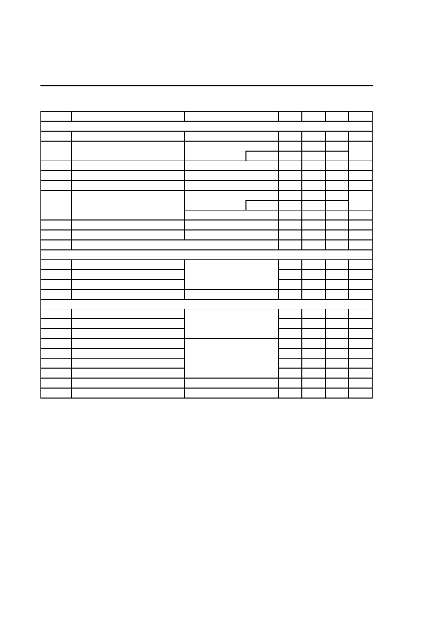
BVDSS
30
V
1
TJ=55°C
5
IGSS
100
nA
VGS(th)
1
1.5
2
V
ID(ON)
100
A
4.9
6.5
TJ=125°C
6.9
8.3
6
7.5
m
gFS
90
S
VSD
0.74
1
V
IS
85
A
Ciss
2100
2520
pF
Coss
536
pF
Crss
165
231
pF
Rg
0.5
0.95
1.5
Qg(4.5V)
19.7
24
nC
Qgs
3.6
4.6
nC
Qgd
7.9
nC
tD(on)
5.9
10
ns
tr
11
17
ns
tD(off)
36.2
55
ns
tf
12
18
ns
trr
35
42
ns
Qrr
33
50
nC
Continuous Drain Current
TC=25°C
TC=100°C
THIS PRODUCT HAS BEEN DESIGNED AND QUALIFIED FOR THE CONSUMER MARKET. APPLICATIONS OR USES AS CRITICAL
COMPONENTS IN LIFE SUPPORT DEVICES OR SYSTEMS ARE NOT AUTHORIZED. AOS DOES NOT ASSUME ANY LIABILITY ARISING
OUT OF SUCH APPLICATIONS OR USES OF ITS PRODUCTS. AOS RESERVES THE RIGHT TO IMPROVE PRODUCT DESIGN,
FUNCTIONS AND RELIABILITY WITHOUT NOTICE
Gate Drain Charge
VGS=0V, VDS=15V, f=1MHz
SWITCHING PARAMETERS
Total Gate Charge
Gate Source Charge
Gate resistance
VGS=0V, VDS=0V, f=1MHz
VGS=4.5V, VDS=15V, ID=20A
Turn-On Rise Time
Turn-Off DelayTime
VGS=10V, VDS=15V, RL=0.75,
RGEN=3
Turn-Off Fall Time
Turn-On DelayTime
m
VGS=4.5V, ID=20A
IS=1A,VGS=0V
VDS=5V, ID=20A
Maximum Body-Diode Continuous Current
Input Capacitance
Output Capacitance
DYNAMIC PARAMETERS
RDS(ON)
Static Drain-Source On-Resistance
Forward Transconductance
Diode Forward Voltage
IDSS
A
Gate Threshold Voltage
VDS=VGS ID=250A
VDS=30V, VGS=0V
VDS=0V, VGS= ±12V
Zero Gate Voltage Drain Current
Gate-Body leakage current
Electrical Characteristics (TJ=25°C unless otherwise noted)
STATIC PARAMETERS
Parameter
Conditions
Body Diode Reverse Recovery Time
Body Diode Reverse Recovery Charge IF=20A, dI/dt=100A/s
Drain-Source Breakdown Voltage
On state drain current
ID=250A, VGS=0V
VGS=10V, VDS=5V
VGS=10V, ID=20A
Reverse Transfer Capacitance
IF=20A, dI/dt=100A/s
A: The value of RθJA is measured with the device in a still air environment with T A =25°C.
B. The power dissipation PD is based on TJ(MAX)=175°C, using junction-to-case thermal resistance, and is more useful in setting the upper
dissipation limit for cases where additional heatsinking is used.
C: Repetitive rating, pulse width limited by junction temperature TJ(MAX)=175°C.
D. The RθJA is the sum of the thermal impedence from junction to case RθJC and case to ambient.
E. The static characteristics in Figures 1 to 6 are obtained using <300
s pulses, duty cycle 0.5% max.
F. These curves are based on the junction-to-case thermal impedence which is measured with the device mounted to a large heatsink,
assuming a maximum junction temperature of TJ(MAX)=175°C.
G. The maximum current rating is limited by bond-wires.
H. These tests are performed with the device mounted on 1 in 2 FR-4 board with 2oz. Copper, in a still air environment with T A=25°C. The
SOA curve provides a single pulse rating.
* This device is guaranteed green after date code 8P11 (June 1
ST 2008)
Rev 5: May 2010
Alpha & Omega Semiconductor, Ltd.
www.aosmd.com
相关PDF资料 |
PDF描述 |
|---|---|
| AOL1712 | 65 A, 30 V, 0.0055 ohm, N-CHANNEL, Si, POWER, MOSFET |
| AOL1718 | 90 A, 30 V, 0.0043 ohm, N-CHANNEL, Si, POWER, MOSFET |
| AON7403 | 29 A, 30 V, 0.018 ohm, P-CHANNEL, Si, POWER, MOSFET |
| AP-454.5 | 410 MHz - 512 MHz MOBILE STATION ANTENNA |
| AP-868U | MOBILE STATION ANTENNA |
相关代理商/技术参数 |
参数描述 |
|---|---|
| AOL1414_10 | 制造商:AOSMD 制造商全称:Alpha & Omega Semiconductors 功能描述:N-Channel Enhancement Mode Field Effect Transistor |
| AOL1414L | 制造商:AOSMD 制造商全称:Alpha & Omega Semiconductors 功能描述:N-Channel Enhancement Mode Field Effect Transistor |
| AOL1418 | 功能描述:MOSFET N-CH 30V 85A ULTRA SO-8 RoHS:是 类别:分离式半导体产品 >> FET - 单 系列:- 标准包装:1,000 系列:MESH OVERLAY™ FET 型:MOSFET N 通道,金属氧化物 FET 特点:逻辑电平门 漏极至源极电压(Vdss):200V 电流 - 连续漏极(Id) @ 25° C:18A 开态Rds(最大)@ Id, Vgs @ 25° C:180 毫欧 @ 9A,10V Id 时的 Vgs(th)(最大):4V @ 250µA 闸电荷(Qg) @ Vgs:72nC @ 10V 输入电容 (Ciss) @ Vds:1560pF @ 25V 功率 - 最大:40W 安装类型:通孔 封装/外壳:TO-220-3 整包 供应商设备封装:TO-220FP 包装:管件 |
| AOL1418L | 制造商:AOSMD 制造商全称:Alpha & Omega Semiconductors 功能描述:N-Channel Enhancement Mode Field Effect Transistor |
| AOL1420 | 制造商:AOSMD 制造商全称:Alpha & Omega Semiconductors 功能描述:N-Channel Enhancement Mode Field Effect Transistor |
发布紧急采购,3分钟左右您将得到回复。