- 您现在的位置:买卖IC网 > PDF目录1779 > AOZ5006QI (Alpha & Omega Semiconductor Inc)IC REG BUCK SYNC ADJ 35A 40QFN PDF资料下载
参数资料
| 型号: | AOZ5006QI |
| 厂商: | Alpha & Omega Semiconductor Inc |
| 文件页数: | 3/16页 |
| 文件大小: | 0K |
| 描述: | IC REG BUCK SYNC ADJ 35A 40QFN |
| 标准包装: | 3,000 |
| 类型: | 降压(降压) |
| 输出类型: | 可调式 |
| 输出数: | 1 |
| 输出电压: | 4.5 V ~ 16 V |
| 输入电压: | 4.5 V ~ 16 V |
| 频率 - 开关: | 200kHz ~ 1MHz |
| 电流 - 输出: | 35A |
| 同步整流器: | 是 |
| 工作温度: | -40°C ~ 85°C |
| 安装类型: | 表面贴装 |
| 封装/外壳: | 40-WFQFN 裸露焊盘 |
| 包装: | 带卷 (TR) |
| 供应商设备封装: | 40-QFN(6x6) |
�� �
�
�AOZ5006�
�Pin� Description�
�Pin� Number�
�1�
�2�
�3�
�4�
�5,� 37�
�6�
�7�
�8� to� 14�
�15�
�16� to� 28�
�29� to� 35�
�36�
�38�
�39�
�40�
�Pin� Name�
�SMOD�
�VCIN�
�VDRV�
�BOOT�
�CGND�
�GH�
�VSWH�
�VIN�
�VSWH�
�PGND�
�VSWH�
�GL�
�THDN�
�DISB#�
�PWM�
�Pin� Function�
�Skip� Mode� input.� When� the� pin� is� held� active� low,� Diode� Emulation� or� Skip� Mode� is� enabled� for�
�the� LS� FET.�
�Control� supply� input.� Nominal� 5V.� Can� be� derived� from� the� gate� drive� supply� VDRV� with� an� RC�
�filter� for� noise� bypass.�
�Gate� drive� supply� input.� Nominal� 5V.�
�Gate� drive� supply� for� the� HS� FET.� Nominal� 5V.� The� bootstrap� diode� is� internal� to� the� module.�
�Connect� a� 0.1� ?� F� or� higher� ceramic� capacitor� between� VSWH� node� at� pin� 7.�
�Control� or� analog� ground� for� return� of� control� signals� and� bypass� capacitors.�
�Attached� to� exposed� pad� in� the� driver� section.�
�Gate� of� the� HS� FET.� Used� for� module� testing� during� production.� No� user� connections.�
�Switching� or� the� phase� node� for� bootstrap� capacitor� connection.�
�Power� input� to� the� switching� MOSFETs.� Attached� to� the� HS� FET� drain� tab.�
�Switching� or� the� phase� node� pin.� Not� for� power� connections.�
�Power� ground.� Internally� connected� to� control� GND� of� pin� 37.�
�Switching� or� phase� node� connected� to� source� of� high� side� MOSFET� and� drain� of� the� low� side�
�MOSFET.� Electrically� attached� to� the� LS� FET� drain� tab.�
�Gate� of� the� LS� FET.� Used� for� module� testing� during� production.� No� user� connections.�
�Open� drain� output� of� the� thermal� shutdown� circuit.� Active� low.�
�Disable� pin� for� the� controller.� Both� gates� are� held� active� low� when� DISB#� is� grounded.�
�Pulse� Width� Modulated� Tri� State� input� from� external� controller.�
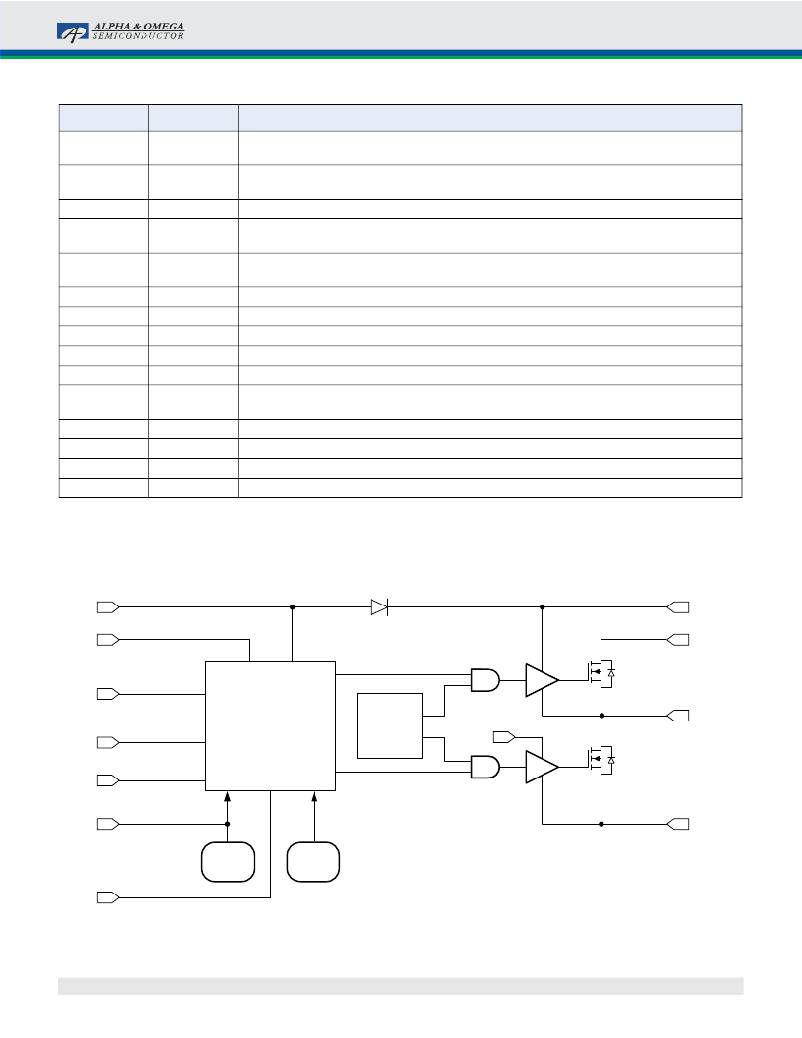
�Functional� Block� Diagram�
�VDRV�
�VCIN�
�PWM�
�BOOT�
�VIN�
�DISB#�
�Complementary�
�Control� Logic�
�Shoot�
�Through�
�Control�
�VDRV�
�VSWH�
�SMOD�
�THDN�
�Temp�
�VCIN�
�PGND�
�CGND�
�SHDN�
�UVLO�
�Rev.� 1.5� April� 2012�
�www.aosmd.com�
�Page� 3� of� 16�
�相关PDF资料 |
PDF描述 |
|---|---|
| AOZ5007QI-01 | IC REG BUCK SYNC ADJ 50A 40QFN |
| AP1084T15L-U | IC REG LDO 1.5V 5A TO220-3 |
| AP1086K33L-13 | IC REG LDO 3.3V 1.5A TO-263 |
| AP1115AYL-13 | IC REG LDO ADJ .6A SOT89-3 |
| AP1117T15L-U | IC REG LDO 1.5V 1A TO220-3 |
相关代理商/技术参数 |
参数描述 |
|---|---|
| AOZ5006QI-01 | 功能描述:IC REG BUCK SYNC ADJ 35A 40QFN RoHS:是 类别:集成电路 (IC) >> PMIC - 稳压器 - DC DC 开关稳压器 系列:- 产品培训模块:Lead (SnPb) Finish for COTS Obsolescence Mitigation Program 标准包装:2,500 系列:- 类型:降压(降压) 输出类型:两者兼有 输出数:1 输出电压:5V,1 V ~ 10 V 输入电压:3.5 V ~ 28 V PWM 型:电流模式 频率 - 开关:220kHz ~ 1MHz 电流 - 输出:600mA 同步整流器:无 工作温度:-40°C ~ 125°C 安装类型:表面贴装 封装/外壳:16-SSOP(0.154",3.90mm 宽) 包装:带卷 (TR) 供应商设备封装:16-QSOP |
| AOZ5007 | 制造商:AOSMD 制造商全称:Alpha & Omega Semiconductors 功能描述:High-Current, High-Performance DrMOS Power Module |
| AOZ5007QI | 功能描述:IC REG BUCK SYNC ADJ 50A 40QFN RoHS:是 类别:集成电路 (IC) >> PMIC - 稳压器 - DC DC 开关稳压器 系列:- 产品培训模块:Lead (SnPb) Finish for COTS Obsolescence Mitigation Program 标准包装:2,500 系列:- 类型:降压(降压) 输出类型:两者兼有 输出数:1 输出电压:5V,1 V ~ 10 V 输入电压:3.5 V ~ 28 V PWM 型:电流模式 频率 - 开关:220kHz ~ 1MHz 电流 - 输出:600mA 同步整流器:无 工作温度:-40°C ~ 125°C 安装类型:表面贴装 封装/外壳:16-SSOP(0.154",3.90mm 宽) 包装:带卷 (TR) 供应商设备封装:16-QSOP |
| AOZ5007QI-01 | 功能描述:IC REG BUCK SYNC ADJ 50A 40QFN RoHS:是 类别:集成电路 (IC) >> PMIC - 稳压器 - DC DC 开关稳压器 系列:- 产品培训模块:Lead (SnPb) Finish for COTS Obsolescence Mitigation Program 标准包装:2,500 系列:- 类型:降压(降压) 输出类型:两者兼有 输出数:1 输出电压:5V,1 V ~ 10 V 输入电压:3.5 V ~ 28 V PWM 型:电流模式 频率 - 开关:220kHz ~ 1MHz 电流 - 输出:600mA 同步整流器:无 工作温度:-40°C ~ 125°C 安装类型:表面贴装 封装/外壳:16-SSOP(0.154",3.90mm 宽) 包装:带卷 (TR) 供应商设备封装:16-QSOP |
| AOZ5019QI | 功能描述:Buck Switching Regulator IC Positive 1 Output 30A 23-VFQFN Exposed Pad 制造商:alpha & omega semiconductor inc. 系列:DrMOS 包装:带卷(TR) 零件状态:有效 功能:降压 输出配置:正 拓扑:降压 输出类型:- 输出数:1 电压 - 输入(最小值):4.5V 电压 - 输入(最大值):25V 电压 - 输出(最小值/固定):- 电压 - 输出(最大值):- 电流 - 输出:30A 频率 - 开关:200kHz ~ 1.5MHz 同步整流器:是 工作温度:-40°C ~ 85°C(TA) 安装类型:表面贴装 封装/外壳:23-VFQFN 裸露焊盘 供应商器件封装:23-QFN(4x4) 标准包装:3,000 |
发布紧急采购,3分钟左右您将得到回复。