- 您现在的位置:买卖IC网 > Datasheet目录203 > AOZ8808DI-05 (Alpha & Omega Semiconductor Inc)TVS DIODE ARRAY LOW CAP 10DFN Datasheet资料下载
参数资料
| 型号: | AOZ8808DI-05 |
| 厂商: | Alpha & Omega Semiconductor Inc |
| 文件页数: | 5/8页 |
| 文件大小: | 0K |
| 描述: | TVS DIODE ARRAY LOW CAP 10DFN |
| 标准包装: | 3,000 |
| 电压 - 反向隔离(标准值): | 5V |
| 电压 - 击穿: | 6V |
| 电极标记: | 4 通道阵列 - 双向 |
| 安装类型: | 表面贴装 |
| 封装/外壳: | 10-UFDFN |
| 供应商设备封装: | 10-DFN |
| 包装: | 带卷 (TR) |
�� �
�
�AOZ8808�
�High� Speed� PCB� Layout� Guidelines�
�Printed� circuit� board� layout� is� the� key� to� achieving� the�
�highest� level� of� surge� immunity� on� power� and� data� lines.�
�The� location� of� the� protection� devices� on� the� PCB� is� the�
�simplest� and� most� important� design� rule� to� follow.� The�
�AOZ8808DI� devices� should� be� located� as� close� as�
�possible� to� the� noise� source.� The� AOZ8808DI� device�
�should� be� placed� on� all� data� and� power� lines� that� enter� or�
�exit� the� PCB� at� the� I/O� connector.� In� most� systems,� surge�
�pulses� occur� on� data� and� power� lines� that� enter� the� PCB�
�through� the� I/O� connector.� Placing� the� AOZ8808DI�
�devices� as� close� as� possible� to� the� noise� source� ensures�
�that� a� surge� voltage� will� be� clamped� before� the� pulse� can�
�be� coupled� into� adjacent� PCB� traces.� In� addition,� the�
�PCB� should� use� the� shortest� possible� traces.� A� short�
�trace� length� equates� to� low� impedance,� which� ensures�
�that� the� surge� energy� will� be� dissipated� by� the�
�AOZ8808DI� device.� Long� signal� traces� will� act� as�
�antennas� to� receive� energy� from� fields� that� are� produced�
�by� the� ESD� pulse.� By� keeping� line� lengths� as� short� as�
�possible,� the� efficiency� of� the� line� to� act� as� an� antenna� for�
�ESD� related� fields� is� reduced.� Minimize� interconnecting�
�line� lengths� by� placing� devices� with� the� most� interconnect�
�as� close� together� as� possible.� The� protection� circuits�
�should� shunt� the� surge� voltage� to� either� the� reference� or�
�chassis� ground.� Shunting� the� surge� voltage� directly� to� the�
�IC’s� signal� ground� can� cause� ground� bounce.� The�
�clamping� performance� of� TVS� diodes� on� a� single� ground�
�PCB� can� be� improved� by� minimizing� the� impedance� with�
�relatively� short� and� wide� ground� traces.� The� PCB� layout�
�and� IC� package� parasitic� inductances� can� cause�
�significant� overshoot� to� the� TVS’s� clamping� voltage.� The�
�inductance� of� the� PCB� can� be� reduced� by� using� short�
�trace� lengths� and� multiple� layers� with� separate� ground�
�and� power� planes.� One� effective� method� to� minimize�
�loop� problems� is� to� incorporate� a� ground� plane� in� the�
�PCB� design.�
�The� AOZ8808DI� ultra-low� capacitance� TVS� is� designed�
�to� protect� four� high� speed� data� transmission� lines� from�
�transient� over-voltages� by� clamping� them� to� a� fixed�
�reference.� The� low� inductance� and� construction�
�minimizes� voltage� overshoot� during� high� current� surges.�
�When� the� voltage� on� the� protected� line� exceeds� the�
�reference� voltage� the� internal� steering� diodes� are� forward�
�biased,� conducting� the� transient� current� away� from� the�
�sensitive� circuitry.� The� AOZ8808DI� is� designed� for� ease�
�of� PCB� layout� by� allowing� the� traces� to� run� underneath�
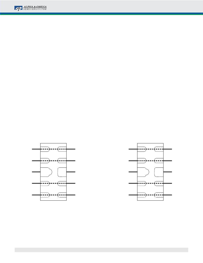
�the� device.� The� pinout� of� the� AOZ8808DI� is� designed� to�
�simply� drop� onto� the� IO� lines� of� a� High� Definition�
�Multimedia� Interface� (HDMI)� or� USB� 3.0� design� without�
�having� to� divert� the� signal� lines� that� may� add� more�
�parasitic� inductance.� Pins� 1,� 2,� 4� and� 5� are� connected� to�
�the� internal� TVS� devices� and� pins� 6,� 7,� 9� and� 10� are� no�
�connects.� The� no� connects� was� done� so� the� package� can�
�be� securely� soldered� onto� the� PCB� surface.�
�Clock�
�Data0�
�Ground�
�Data1�
�Data2�
�Clock�
�Data0�
�Ground�
�Data1�
�Data2�
�SSRX+�
�SSRX–�
�Ground�
�SSTX+�
�SSTX–�
�SSRX+�
�SSRX–�
�Ground�
�SSTX+�
�SSTX–�
�.�
�Figure� 3.� Flow� Through� Layout� for� HDMI�
�Figure� 4.� Flow� Through� Layout� for� USB� 3.0�
�Rev.� 2.1� May� 2012�
�www.aosmd.com�
�Page� 5� of� 8�
�相关PDF资料 |
PDF描述 |
|---|---|
| AOZ8818DI-03 | TVS DIODE ARRAY LOW CAP 10DFN |
| APA1FGRA04 | SWITCH PUSH SPDT 0.05A 48V |
| APBE1FGRA04 | SWITCH PUSH SPDT 0.05A 48V |
| APLVD400 | VOLTMETER AC 3 1/2-DIGIT |
| APMR0016 | MOD APMR 3-PH VAULT DET DIN RAIL |
相关代理商/技术参数 |
参数描述 |
|---|---|
| AOZ8809ADI-03 | 功能描述:TVS DIODE 3.3V 4CH LOW CAP DFN 制造商:alpha & omega semiconductor inc. 系列:- 零件状态:在售 类型:齐纳 单向通道:4 电压 - 反向关态(典型值):3.3V(最大) 电压 - 击穿(最小值):- 电压 - 箝位(最大值)@ Ipp:4V 电流 - 峰值脉冲(10/1000μs):5A 功率 - 峰值脉冲:- 电源线路保护:无 应用:通用 不同频率时的电容:0.45pF @ 1MHz 工作温度:-40°C ~ 125°C (TJ) 安装类型:表面贴装 封装/外壳:3-UFDFN 供应商器件封装:3-DFN(1.0 x 0.60) 标准包装:3,000 |
| AOZ8809ADI-05 | 功能描述:TVS DIODE 5.0V 4CH LOW CAP DFN 制造商:alpha & omega semiconductor inc. 系列:- 零件状态:在售 类型:齐纳 单向通道:4 电压 - 反向关态(典型值):5V(最大) 电压 - 击穿(最小值):- 电压 - 箝位(最大值)@ Ipp:5V 电流 - 峰值脉冲(10/1000μs):5A 功率 - 峰值脉冲:- 电源线路保护:无 应用:通用 不同频率时的电容:0.45pF @ 1MHz 工作温度:-40°C ~ 125°C (TJ) 安装类型:表面贴装 封装/外壳:3-UFDFN 供应商器件封装:3-DFN(1.0 x 0.60) 标准包装:3,000 |
| AOZ8809DI-03 | 功能描述:TVS DIODE 3.3VWM 8VC DFN 制造商:alpha & omega semiconductor inc. 系列:- 包装:剪切带(CT) 零件状态:有效 类型:转向装置(轨至轨) 单向通道:- 双向通道:4 电压 - 反向关态(典型值):3.3V(最大) 电压 - 击穿(最小值):3.5V 电压 - 箝位(最大值)@ Ipp:8V 电流 - 峰值脉冲(10/1000μs):12A(100ns) 功率 - 峰值脉冲:- 电源线路保护:是 应用:HDMI 不同频率时的电容:0.45pF @ 1MHz 工作温度:-40°C ~ 125°C (TJ) 安装类型:表面贴装 封装/外壳:10-UFDFN 供应商器件封装:10-DFN(2.5x1) 标准包装:1 |
| AOZ8809DI-05 | 功能描述:TVS DIODE 5VWM 9VC DFN 制造商:alpha & omega semiconductor inc. 系列:- 包装:剪切带(CT) 零件状态:有效 类型:转向装置(轨至轨) 单向通道:- 双向通道:4 电压 - 反向关态(典型值):5V(最大) 电压 - 击穿(最小值):6V 电压 - 箝位(最大值)@ Ipp:9V 电流 - 峰值脉冲(10/1000μs):12A(100ns) 功率 - 峰值脉冲:- 电源线路保护:是 应用:HDMI 不同频率时的电容:0.45pF @ 1MHz 工作温度:-40°C ~ 125°C (TJ) 安装类型:表面贴装 封装/外壳:10-UFDFN 供应商器件封装:10-DFN(2.5x1) 标准包装:1 |
| AOZ8811 | 制造商:AOSMD 制造商全称:Alpha & Omega Semiconductors 功能描述:Ultra-Low Capacitance One-line TVS Diode |
发布紧急采购,3分钟左右您将得到回复。