- 您现在的位置:买卖IC网 > PDF目录166221 > AP1202HS (INTEGRATED CIRCUIT TECHNOLOGY CORP) 0.6 A HALF BRDG BASED MOSFET DRIVER, PDSO8 PDF资料下载
参数资料
| 型号: | AP1202HS |
| 厂商: | INTEGRATED CIRCUIT TECHNOLOGY CORP |
| 元件分类: | MOSFETs |
| 英文描述: | 0.6 A HALF BRDG BASED MOSFET DRIVER, PDSO8 |
| 封装: | SOIC-8 |
| 文件页数: | 5/11页 |
| 文件大小: | 702K |
| 代理商: | AP1202HS |
AP1202
Dual USB High-Side Power Switch
Anachip Corp.
www.anachip.com.tw
Rev 1.1 May.26, 2005
3/11
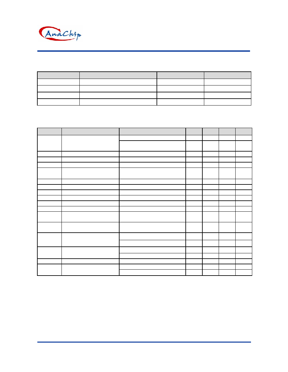
Operating Ratings (Note 2)
Symbol
Parameter
Rating
Unit
VIN
Supply Voltage
+2.7 to +5.5
V
TA
Ambient Operating Temperature
-40 to +85
oC
ΘJA
Thermal Resistance SOIC
120
oC/W
ΘJA
Thermal Resistance DIP
100
oC/W
Electrical Characteristics (Under Operating Conditions) V
IN=+5V; TA=25
oC; unless noted.
Symbol
Parameter
Conditions
Min.
Typ.
Max.
Unit
switch off, OUT = open (Note 4)
-
0.50
5
A
ICC
Supply Current
all switches on, OUT = open
(Note 4)
-
110
160
A
VIT
Enable Input Threshold
(Note 4)
0.8
1.7
2.40
V
IEN
Enable Input Current
VEN =0V to 5.5V
-1
±0.01
1
A
CEN
Enable Input Capacitance
-
1
-
pF
RDS(ON)
Switch Resistance
VIN =2.7V ~ 5.5V, IOUT =500mA,
each switch
-
110
140
m
TOND
Output Turn-On Delay
RL =10 each output
-
30
-
S
TR
Output Turn-On Rise Time
RL =10 each output
-
1
-
mS
TOFFD
Output Turnoff Delay
RL =10 each output
-
0.5
10
S
TF
Output Turnoff Fall Time
RL =10 each output
-
0.5
10
S
ILEAK
Output Leakage Current
each output (output disabled)
-
10
A
IOUT
Continuous Load Current
each output
0.6
-
A
IOS
Short-circuit Current Limit
Each output (enable), output
into 1
-
0.6
0.7
A
ILIM
Current-Limit Threshold
Ramped load applied to
enabled output
0.60
0.75
0.90
A
TJ increasing
-
140
-
oC
TTS
Over-temperature
Shutdown Threshold
TJ decreasing
-
130
-
oC
VIN = 5V, IL = 10mA
-
10
25
RFO
Error Flag Output
Resistance
VIN = 3.3V, IL = 10mA
-
15
40
IFOH
Error Flag Off Current
VFLAG = 5V
-
0.01
1
A
VIN = increasing
-
2.5
-
V
UVLO
UVLO Threshold
VIN = decreasing
-
2.3
-
V
Note 1. Exceeding the absolute maximum rating may damage the device.
Note 2. The device is not guaranteed to function outside its operating rating.
Note 3. Devices are ESD sensitive. Handling precautions recommended. Human body model, 1.5k in series with 100pF.
Note 4. Off is VEN≦0.8Vand on is VEN≧2.4V for the AP1202H. Off is VEN≧2.4V and on is VEN≦0.8V for the AP1202L.
相关PDF资料 |
PDF描述 |
|---|---|
| AP1202LNL | 0.6 A HALF BRDG BASED MOSFET DRIVER, PDIP8 |
| AP1202LN | 0.6 A HALF BRDG BASED MOSFET DRIVER, PDIP8 |
| AP1202LSA | 0.6 A HALF BRDG BASED MOSFET DRIVER, PDSO8 |
| AP1202LSLA | 0.6 A HALF BRDG BASED MOSFET DRIVER, PDSO8 |
| AP1202LSL | 0.6 A HALF BRDG BASED MOSFET DRIVER, PDSO8 |
相关代理商/技术参数 |
参数描述 |
|---|---|
| AP1202HSA | 制造商:ANACHIP 制造商全称:Anachip Corp 功能描述:Dual USB High-Side Power Switch |
| AP1202HSL | 制造商:ANACHIP 制造商全称:Anachip Corp 功能描述:Dual USB High-Side Power Switch |
| AP1202HSLA | 制造商:ANACHIP 制造商全称:Anachip Corp 功能描述:Dual USB High-Side Power Switch |
| AP1202LN | 制造商:ANACHIP 制造商全称:Anachip Corp 功能描述:Dual USB High-Side Power Switch |
| AP1202LNA | 制造商:ANACHIP 制造商全称:Anachip Corp 功能描述:Dual USB High-Side Power Switch |
发布紧急采购,3分钟左右您将得到回复。