参数资料
| 型号: | AP7217A-33SPG-13 |
| 厂商: | Diodes Inc |
| 文件页数: | 7/10页 |
| 文件大小: | 0K |
| 描述: | IC REG LDO 3.3V .6A 8-SOIC |
| 标准包装: | 2,500 |
| 稳压器拓扑结构: | 正,固定式 |
| 输出电压: | 3.3V |
| 输入电压: | 最高 5.5V |
| 电压 - 压降(标准): | 0.8V @ 600mA |
| 稳压器数量: | 1 |
| 电流 - 输出: | 600mA(最小值) |
| 工作温度: | -40°C ~ 85°C |
| 安装类型: | 表面贴装 |
| 封装/外壳: | 8-SOIC(0.154",3.90mm Width)裸露焊盘 |
| 供应商设备封装: | 8-SOP-EP |
| 包装: | 带卷 (TR) |
�� �
�
�AP7217A�
�3.3V� 600mA� CMOS� LDO�
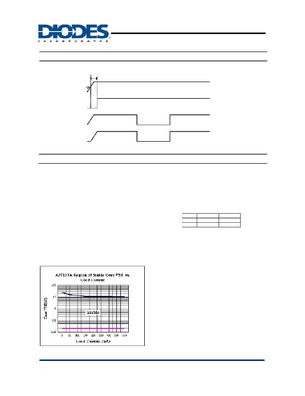
�Timing� Diagram�
�t� RP�
�200mSec-TYP.�
�1.6V�
�V� IN�
�VD� OUT�
�EN�
�VR� OUT�
�Application� Note�
�Input� Capacitor�
�A� 1� μ� F� ceramic� capacitor� is� recommended� to� connect� between� IN�
�and� GND� pins� to� decouple� input� power� supply� glitch� and� noise.�
�The� amount� of� the� capacitance� may� be� increased� without� limit.� A�
�lower� ESR� (Equivalent� Series� Resistance)� capacitor� allows� the�
�use� of� less� capacitance,� while� higher� ESR� type� requires� more�
�capacitance.� This� input� capacitor� must� be� located� as� close� as�
�possible� to� the� device� to� assure� input� stability� and� less� noise.� For�
�PCB� layout,� a� wide� copper� trace� is� required� for� both� IN� and� GND.�
�ENABLE/SHUTDOWN� Operation�
�The� AP7217A� is� turned� on� by� setting� the� EN� pin� high,� and� is�
�turned� off� by� pulling� it� low.� If� this� feature� is� not� used,� the� EN� pin�
�should� be� tied� to� IN� pin� to� keep� the� regulator� output� on� at� all� time.�
�To� ensure� proper� operation,� the� signal� source� used� to� drive� the�
�EN� pin� must� be� able� to� swing� above� and� below� the� specified�
�turn-on/off� voltage� thresholds� listed� in� the� Electrical�
�Characteristics� section� under� V� IL� and� V� IH� .�
�VR� OUT�
�VD� OUT�
�Output� Capacitor�
�The� output� capacitor� is� required� to� stabilize� and� help� the� transient�
�EN=0�
�EN=1�
�0V�
�3.3V�
�Φ�
�Φ�
�response� of� the� LDO.� The� AP7217A� is� designed� to� have�
�excellent� transient� response� for� most� applications� with� a� small�
�amount� of� output� capacitance.� The� AP7217� is� stable� with� any�
�small� ceramic� output� capacitors� of� 1.0� μ� F� or� higher� value,� and� the�
�temperature� coefficients� of� X7R� or� X5R� type.� Additional�
�capacitance� helps� to� reduce� undershoot� and� overshoot� during�
�transient.� For� PCB� layout,� the� output� capacitor� must� be� placed� as�
�close� as� possible� to� OUT� and� GND� pins,� and� keep� the� leads� as�
�short� as� possible.�
�Thermal� Considerations�
�Thermal� Shutdown� Protection� limits� power� dissipation� in�
�AP7217A.� When� the� operation� junction� temperature� exceeds�
�150°C,� the� Over� Temperature� Protection� circuit� starts� the� thermal�
�shutdown� function� and� turns� the� pass� element� off.� The� pass�
�element� turn� on� again� after� the� junction� temperature� cools� by�
�40°C.� For� continuous� operation,� do� not� exceed� absolute�
�maximum� operation� junction� temperature� 125°C.� The� power�
�dissipation� definition� in� device� is:�
�P� D� =� (V� IN� ?� V� OU� T)� x� I� OUT� +� V� IN� x� I� Q�
�The� maximum� power� dissipation� depends� on� the� thermal�
�resistance� of� IC� package,� PCB� layout,� the� rate� of� surroundings�
�airflow� and� temperature� difference� between� junction� to� ambient.�
�The� maximum� power� dissipation� can� be� calculated� by� following�
�formula� :�
�P� D(MAX)� =� (� T� J(MAX)� -� TA� )� /� θ� JA�
�Where� T� J(MAX)� is� the� maximum� operation� junction� temperature�
�125°C,� T� A� is� the� ambient� temperature� and� the� θ� JA� is� the� junction�
�to� ambient� thermal� resistance.�
�AP7217A� Rev.� 3�
�DS31423�
�7� of� 10�
��OCTOBER� 2009�
�?� Diodes� Incorporated�
�相关PDF资料 |
PDF描述 |
|---|---|
| EGM28DTMT-S189 | CONN EDGECARD 56POS R/A .156 SLD |
| MC7812CDTG | IC REG LDO 12V 1A DPAK-3 |
| MC7805CDTG | IC REG LDO 5V 1A DPAK |
| GMM30DTMS | CONN EDGECARD 60POS R/A .156 SLD |
| GMM28DRAN | CONN EDGECARD 56POS R/A .156 SLD |
相关代理商/技术参数 |
参数描述 |
|---|---|
| AP7217A-33SPG-U | 制造商:DIODES 制造商全称:Diodes Incorporated 功能描述:3.3V 600mA CMOS LDO |
| AP7217C | 制造商:DIODES 制造商全称:Diodes Incorporated 功能描述:1.25V 600mA CMOS LDO |
| AP7217C-13SPG-13 | 功能描述:低压差稳压器 - LDO LDO 1.25V 600mA CMOS 550MA 0.35V 2.5-5.5V RoHS:否 制造商:Texas Instruments 最大输入电压:36 V 输出电压:1.4 V to 20.5 V 回动电压(最大值):307 mV 输出电流:1 A 负载调节:0.3 % 输出端数量: 输出类型:Fixed 最大工作温度:+ 125 C 安装风格:SMD/SMT 封装 / 箱体:VQFN-20 |
| AP7217D | 制造商:DIODES 制造商全称:Diodes Incorporated 功能描述:1.2V 600mA CMOS LDO |
| AP7217D-12YG-13 | 功能描述:低压差稳压器 - LDO LDO 600mA 2.5-5.5V 0.8V RoHS:否 制造商:Texas Instruments 最大输入电压:36 V 输出电压:1.4 V to 20.5 V 回动电压(最大值):307 mV 输出电流:1 A 负载调节:0.3 % 输出端数量: 输出类型:Fixed 最大工作温度:+ 125 C 安装风格:SMD/SMT 封装 / 箱体:VQFN-20 |
发布紧急采购,3分钟左右您将得到回复。