参数资料
| 型号: | APA150-FGG144A |
| 厂商: | Microsemi SoC |
| 文件页数: | 57/178页 |
| 文件大小: | 0K |
| 描述: | IC FPGA PROASIC+ 150K 144-FBGA |
| 标准包装: | 160 |
| 系列: | ProASICPLUS |
| RAM 位总计: | 36864 |
| 输入/输出数: | 100 |
| 门数: | 150000 |
| 电源电压: | 2.375 V ~ 2.625 V |
| 安装类型: | 表面贴装 |
| 工作温度: | -40°C ~ 125°C |
| 封装/外壳: | 144-LBGA |
| 供应商设备封装: | 144-FPBGA(13x13) |
第1页第2页第3页第4页第5页第6页第7页第8页第9页第10页第11页第12页第13页第14页第15页第16页第17页第18页第19页第20页第21页第22页第23页第24页第25页第26页第27页第28页第29页第30页第31页第32页第33页第34页第35页第36页第37页第38页第39页第40页第41页第42页第43页第44页第45页第46页第47页第48页第49页第50页第51页第52页第53页第54页第55页第56页当前第57页第58页第59页第60页第61页第62页第63页第64页第65页第66页第67页第68页第69页第70页第71页第72页第73页第74页第75页第76页第77页第78页第79页第80页第81页第82页第83页第84页第85页第86页第87页第88页第89页第90页第91页第92页第93页第94页第95页第96页第97页第98页第99页第100页第101页第102页第103页第104页第105页第106页第107页第108页第109页第110页第111页第112页第113页第114页第115页第116页第117页第118页第119页第120页第121页第122页第123页第124页第125页第126页第127页第128页第129页第130页第131页第132页第133页第134页第135页第136页第137页第138页第139页第140页第141页第142页第143页第144页第145页第146页第147页第148页第149页第150页第151页第152页第153页第154页第155页第156页第157页第158页第159页第160页第161页第162页第163页第164页第165页第166页第167页第168页第169页第170页第171页第172页第173页第174页第175页第176页第177页第178页
ProASICPLUS Flash Family FPGAs
v5.9
2-5
Array Coordinates
During many place-and-route operations in Actel’s
Designer software tool, it is possible to set constraints
that require array coordinates.
Table 2-2 is provided as a reference. The array coordinates
are measured from the lower left (0,0). They can be used in
region constraints for specific groups of core cells, I/Os, and
RAM blocks. Wild cards are also allowed.
I/O and cell coordinates are used for placement
constraints. Two coordinate systems are needed because
there is not a one-to-one correspondence between I/O
cells and core cells. In addition, the I/O coordinate system
changes depending on the die/package combination.
Core cell coordinates start at the lower left corner
(represented as (1,1)) or at (1,5) if memory blocks are
present at the bottom. Memory coordinates use the
same system and are indicated in Table 2-2. The memory
coordinates for an APA1000 are illustrated in Figure 2-5.
For more information on how to use constraints, see the
Designer User’s Guide or online help for ProASICPLUS
software tools.
Table 2-2
Array Coordinates
Device
Logic Tile
Memory Rows
All
Min.
Max.
Bottom
Top
xy
x
y
Min.
Max.
APA075
1
96
32
–
(33,33) or (33, 35)
0,0
97, 37
APA150
1
128
48
–
(49,49) or (49, 51)
0,0
129, 53
APA300
1
5
128
68
(1,1) or (1,3)
(69,69) or (69, 71)
0,0
129, 73
APA450
1
5
192
68
(1,1) or (1,3)
(69,69) or (69, 71)
0,0
193, 73
APA600
1
5
224
100
(1,1) or (1,3)
(101,101) or (101, 103)
0,0
225, 105
APA750
1
5
256
132
(1,1) or (1,3)
(133,133) or (133, 135)
0,0
257, 137
APA1000
1
5
352
164
(1,1) or (1,3)
(165,165) or (165, 167)
0,0
353, 169
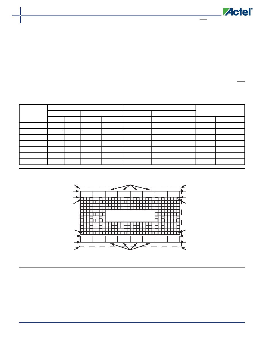
Figure 2-5 Core Cell Coordinates for the APA1000
(353,169)
(352,167)
(352,165)
(352,164)
(352,5)
(352,3)
(353,0)
(352,1)
(1,5)
(1,1)
(1,164)
(1,165)
(1,3)
(1,167)
(1,169)
(0,0)
Core
Memory
Blocks
Memory
Blocks
相关PDF资料 |
PDF描述 |
|---|---|
| APA150-FG144A | IC FPGA PROASIC+ 150K 144-FBGA |
| A54SX16A-FG256 | IC FPGA SX 24K GATES 256-FBGA |
| A54SX16A-FGG256 | IC FPGA SX 24K GATES 256-FBGA |
| EP4CE30F29I7N | IC CYCLONE IV FPGA 30K 780FBGA |
| EP4CE30F29C6N | IC CYCLONE IV FPGA 30K 780FBGA |
相关代理商/技术参数 |
参数描述 |
|---|---|
| APA150-FGG144I | 功能描述:IC FPGA PROASIC+ 150K 144-FBGA RoHS:是 类别:集成电路 (IC) >> 嵌入式 - FPGA(现场可编程门阵列) 系列:ProASICPLUS 标准包装:40 系列:SX-A LAB/CLB数:6036 逻辑元件/单元数:- RAM 位总计:- 输入/输出数:360 门数:108000 电源电压:2.25 V ~ 5.25 V 安装类型:表面贴装 工作温度:0°C ~ 70°C 封装/外壳:484-BGA 供应商设备封装:484-FPBGA(27X27) |
| APA150-FGG256 | 功能描述:IC FPGA PROASIC+ 150K 256-FBGA RoHS:是 类别:集成电路 (IC) >> 嵌入式 - FPGA(现场可编程门阵列) 系列:ProASICPLUS 标准包装:90 系列:ProASIC3 LAB/CLB数:- 逻辑元件/单元数:- RAM 位总计:36864 输入/输出数:157 门数:250000 电源电压:1.425 V ~ 1.575 V 安装类型:表面贴装 工作温度:-40°C ~ 125°C 封装/外壳:256-LBGA 供应商设备封装:256-FPBGA(17x17) |
| APA150-FGG256A | 功能描述:IC FPGA PROASIC+ 150K 256-FBGA RoHS:是 类别:集成电路 (IC) >> 嵌入式 - FPGA(现场可编程门阵列) 系列:ProASICPLUS 标准包装:90 系列:ProASIC3 LAB/CLB数:- 逻辑元件/单元数:- RAM 位总计:36864 输入/输出数:157 门数:250000 电源电压:1.425 V ~ 1.575 V 安装类型:表面贴装 工作温度:-40°C ~ 125°C 封装/外壳:256-LBGA 供应商设备封装:256-FPBGA(17x17) |
| APA150-FGG256I | 功能描述:IC FPGA PROASIC+ 150K 256-FBGA RoHS:是 类别:集成电路 (IC) >> 嵌入式 - FPGA(现场可编程门阵列) 系列:ProASICPLUS 标准包装:40 系列:SX-A LAB/CLB数:6036 逻辑元件/单元数:- RAM 位总计:- 输入/输出数:360 门数:108000 电源电压:2.25 V ~ 5.25 V 安装类型:表面贴装 工作温度:0°C ~ 70°C 封装/外壳:484-BGA 供应商设备封装:484-FPBGA(27X27) |
| APA150-FGGB | 制造商:ACTEL 制造商全称:Actel Corporation 功能描述:ProASIC Flash Family FPGAs |
发布紧急采购,3分钟左右您将得到回复。