- 您现在的位置:买卖IC网 > PDF目录36715 > APT5017SVFRG (MICROSEMI POWER PRODUCTS GROUP) 30 A, 500 V, 0.17 ohm, N-CHANNEL, Si, POWER, MOSFET PDF资料下载
参数资料
| 型号: | APT5017SVFRG |
| 厂商: | MICROSEMI POWER PRODUCTS GROUP |
| 元件分类: | JFETs |
| 英文描述: | 30 A, 500 V, 0.17 ohm, N-CHANNEL, Si, POWER, MOSFET |
| 封装: | D3PAK-3 |
| 文件页数: | 2/4页 |
| 文件大小: | 63K |
| 代理商: | APT5017SVFRG |
050-7403
Rev
D
2-2004
APT40GP60B_S
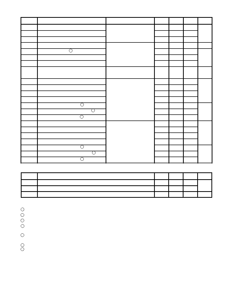
DYNAMIC CHARACTERISTICS
Symbol
Cies
Coes
Cres
VGEP
Qg
Qge
Qgc
SSOA
td(on)
tr
td(off)
tf
Eon1
Eon2
Eoff
td(on)
tr
td(off)
tf
Eon1
Eon2
Eoff
Test Conditions
Capacitance
VGE = 0V, VCE = 25V
f = 1 MHz
Gate Charge
VGE = 15V
VCE = 300V
IC = 40A
TJ = 150°C, RG = 5, VGE =
15V, L = 100H,VCE = 600V
Inductive Switching (25°C)
VCC(Peak) = 400V
VGE = 15V
IC = 40A
RG = 5
TJ = +25°C
Inductive Switching (125°C)
VCC(Peak) = 400V
VGE = 15V
IC = 40A
RG = 5
TJ = +125°C
Characteristic
Input Capacitance
Output Capacitance
Reverse Transfer Capacitance
Gate-to-Emitter Plateau Voltage
Total Gate Charge 3
Gate-Emitter Charge
Gate-Collector ("Miller ") Charge
Switching SOA
Turn-on Delay Time
Current Rise Time
Turn-off Delay Time
Current Fall Time
Turn-on Switching Energy 4
Turn-on Switching Energy (Diode) 5
Turn-off Switching Energy 6
Turn-on Delay Time
Current Rise Time
Turn-off Delay Time
Current Fall Time
Turn-on Switching Energy 4
Turn-on Switching Energy (Diode) 5
Turn-off Switching Energy 6
MIN
TYP
MAX
4610
395
25
7.5
135
30
40
160
20
29
64
45
385
644
352
450
20
29
89
69
385
972
615
950
UNIT
pF
V
nC
A
ns
J
ns
J
UNIT
°C/W
gm
MIN
TYP
MAX
.23
N/A
5.90
Characteristic
Junction to Case (IGBT)
Junction to Case (DIODE)
Package Weight
Symbol
RΘJC
WT
THERMAL AND MECHANICAL CHARACTERISTICS
1 Repetitive Rating: Pulse width limited by maximum junction temperature.
2 For Combi devices, I
ces
includes both IGBT and FRED leakages
3 See MIL-STD-750 Method 3471.
4E
on1
is the clamped inductive turn-on-energy of the IGBT only, without the effect of a commutating diode reverse recovery current
adding to the IGBT turn-on loss. (See Figure24.)
5E
on2
is the clamped inductive turn-on energy that includes a commutating diode reverse recovery current in the IGBT turn-on switching
loss. A Combi device is used for the clamping diode as shown in the E
on2
test circuit. (See Figures 21, 22.)
6E
off
is the clamped inductive turn-off energy measured in accordance wtih JEDEC standard JESD24-1. (See Figures 21, 23.)
7 Continuous current limited by package lead temperature.
APT Reserves the right to change, without notice, the specifications and information contained herein.
相关PDF资料 |
PDF描述 |
|---|---|
| APT5017BVFR | 30 A, 500 V, 0.17 ohm, N-CHANNEL, Si, POWER, MOSFET, TO-247AD |
| APT5017BVFR | 30 A, 500 V, 0.17 ohm, N-CHANNEL, Si, POWER, MOSFET, TO-247AD |
| APT5017BVRG | 30 A, 500 V, 0.17 ohm, N-CHANNEL, Si, POWER, MOSFET, TO-247 |
| APT5017BVR | 30 A, 500 V, 0.17 ohm, N-CHANNEL, Si, POWER, MOSFET, TO-247 |
| APT5017BVR | 30 A, 500 V, 0.17 ohm, N-CHANNEL, Si, POWER, MOSFET, TO-247 |
相关代理商/技术参数 |
参数描述 |
|---|---|
| APT5017SVR | 制造商:ADPOW 制造商全称:Advanced Power Technology 功能描述:Power MOS V is a new generation of high voltage N-Channel enhancement mode power MOSFETs. |
| APT5017SVRG | 功能描述:MOSFET N-CH 500V 30A D3PAK RoHS:是 类别:分离式半导体产品 >> FET - 单 系列:POWER MOS V® 标准包装:1,000 系列:MESH OVERLAY™ FET 型:MOSFET N 通道,金属氧化物 FET 特点:逻辑电平门 漏极至源极电压(Vdss):200V 电流 - 连续漏极(Id) @ 25° C:18A 开态Rds(最大)@ Id, Vgs @ 25° C:180 毫欧 @ 9A,10V Id 时的 Vgs(th)(最大):4V @ 250µA 闸电荷(Qg) @ Vgs:72nC @ 10V 输入电容 (Ciss) @ Vds:1560pF @ 25V 功率 - 最大:40W 安装类型:通孔 封装/外壳:TO-220-3 整包 供应商设备封装:TO-220FP 包装:管件 |
| APT5018BFLL | 制造商:ADPOW 制造商全称:Advanced Power Technology 功能描述:Power MOS 7TM is a new generation of low loss, high voltage, N-Channel enhancement mode power MOSFETS |
| APT5018BFLL_03 | 制造商:ADPOW 制造商全称:Advanced Power Technology 功能描述:POWER MOS 7 FREDFET |
| APT5018BFLLG | 功能描述:MOSFET N-CH 500V 27A TO-247 RoHS:是 类别:分离式半导体产品 >> FET - 单 系列:POWER MOS 7® 标准包装:1,000 系列:MESH OVERLAY™ FET 型:MOSFET N 通道,金属氧化物 FET 特点:逻辑电平门 漏极至源极电压(Vdss):200V 电流 - 连续漏极(Id) @ 25° C:18A 开态Rds(最大)@ Id, Vgs @ 25° C:180 毫欧 @ 9A,10V Id 时的 Vgs(th)(最大):4V @ 250µA 闸电荷(Qg) @ Vgs:72nC @ 10V 输入电容 (Ciss) @ Vds:1560pF @ 25V 功率 - 最大:40W 安装类型:通孔 封装/外壳:TO-220-3 整包 供应商设备封装:TO-220FP 包装:管件 |
发布紧急采购,3分钟左右您将得到回复。