- 您现在的位置:买卖IC网 > PDF目录381303 > AS1106WL-T (AUSTRIAMICROSYSTEMS AG) 8-digit, 5mA, serial Int.; Package Type: SOIC-24; Temperature Range: 0 - +70 °C PDF资料下载
参数资料
| 型号: | AS1106WL-T |
| 厂商: | AUSTRIAMICROSYSTEMS AG |
| 元件分类: | LED驱动器 |
| 英文描述: | 8-digit, 5mA, serial Int.; Package Type: SOIC-24; Temperature Range: 0 - +70 °C |
| 中文描述: | LED DISPLAY DRIVER, PDSO24 |
| 封装: | SOIC-24 |
| 文件页数: | 13/21页 |
| 文件大小: | 829K |
| 代理商: | AS1106WL-T |
13 - 21
AS1106, AS1107
Datasheet - Detailed Description
8.5.6 Feature Register
(0xXE)
The Feature Register is used for enabling various features including switching the device into external clock mode, applying an external reset,
selecting code-B or HEX decoding, enabling or disabling blinking, enabling or disabling the SPI-compatible interface (AS1106 only), setting the
blinking rate, and resetting the blink timng.
Note:
At power-up the Feature Register is initialized to 0.
8.5.7 No-Op Register (0xX0)
The No-Op Register is used when multiple AS1106 or AS1107 devices are cascaded in order to support displays with more than 8 digits. The
cascading must be done in such a way that all DOUT pins are connected to DIN of the next AS1106/AS1107 (see Figure 14 on page 16). The
LOAD/CSN and CLK signals are connected to all devices.
For example, if five devices are cascaded, in order to performa write operation to the fifth device, the write-command must be followed by four
no-operation commands. When the LOAD/CSN signal goes high, all shift registers are latched. The first four devices will receive no-operation
commands and only the fifth device will receive the intended operation command, and subsequently update its register.
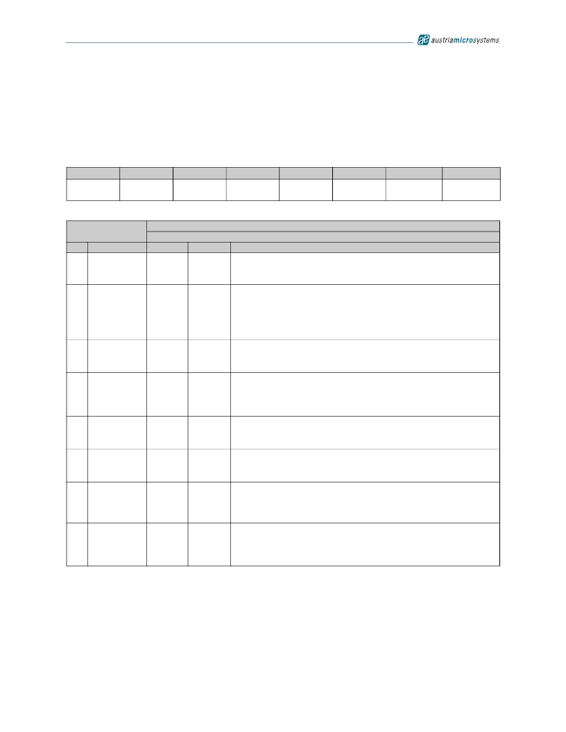
Table 17. Feature Register Summary
D7
blink_
start
D6
D5
blink_
freq_sel
D4
D3
D2
D1
D0
sync
blink_en
spi_en
decode_sel
reg_res
clk_en
Table 18. Feature Register Bit Descriptions (Address (HEX) = 0xXE))
Feature Register
Enables and disables various device features.
Bit
Bit Name
Default
Addr: 0xXE
Access
Bit Description
D0
clk_en
0
R/W
External clock active.
0 = Internal oscillator is used for systemclock.
1 = Pin CLK of the serial interface operates as systemclock input.
Resets all control registers except the Feature Register.
0 = Reset Disabled. Normal operation.
1 = All control registers are reset to default state (except the Feature Register)
identically after power-up.
Note:
The Digit Registers maintain their data.
Selects display decoding.
0 = Enable Code-B decoding (see Table10 on page10).
1 = Enable HEX decoding (see Table11 on page11).
Enables the SPI-compatible interface.
0 = Disable SPI-compatible interface (AS1106 only).
1 = Enable the SPI-compatible interface (AS1106 only).
Note:
The SPI-compatible interface is always enabled in the AS1107.
Enables blinking.
0 = Disable blinking.
1 = Enable blinking.
Sets blink with low frequency (with the internal oscillator enabled):
0 = Blink period typically is 1 second (0.5s on, 0.5s off).
1 = Blink period is 2 seconds (1s on, 1s off).
Synchronizes blinking on the rising edge of pin LOAD/CSN. The multiplex and blink
timng counter is cleared on the rising edge of pin LOAD/CSN. By setting this bit in
multiple AS1106/AS1107 devices, the blink timng can be synchronized across all the
devices.
Start Blinking with display enabled phase. When bit D4 (blink_en) is set, bit D7
determnes how blinking starts.
0 = Blinking starts with the display turned off.
1 = Blinking starts with the display turned on.
D1
reg_res
0
R/W
D2
decode_sel
0
R/W
D3
spi_en
0
R/W
D4
blink_en
0
R/W
D5
blink_freq_sel
0
R/W
D6
sync
0
R/W
D7
blink_start
0
R/W
相关PDF资料 |
PDF描述 |
|---|---|
| AS1108PL | 4-digit, 5mA, serial Int.; Package Type: PDIP-20; Temperature Range: 0 - +70 °C |
| AS1108WL-T | 4-digit, 5mA, serial Int.; Package Type: SOIC-20; Temperature Range: 0 - +70 °C |
| AS1109-BQFT | 100mA, 8-Bit, Diagnostic; Package Type: QFN(4x4)-16 |
| AS1109-BSOT | 100mA, 8-Bit, Diagnostic |
| AS1109-BSST | 100mA, 8-Bit, Diagnostic; Package Type: SSOP-16 |
相关代理商/技术参数 |
参数描述 |
|---|---|
| AS1106-XXX-I-A1-D | 制造商:未知厂家 制造商全称:未知厂家 功能描述:Analog Filter |
| AS1106-XXX-I-A1-S | 制造商:未知厂家 制造商全称:未知厂家 功能描述:Analog Filter |
| AS1106-XXX-I-A2-D | 制造商:未知厂家 制造商全称:未知厂家 功能描述:Analog Filter |
| AS1106-XXX-I-A2-S | 制造商:未知厂家 制造商全称:未知厂家 功能描述:Analog Filter |
| AS1106-XXX-I-A3-D | 制造商:未知厂家 制造商全称:未知厂家 功能描述:Analog Filter |
发布紧急采购,3分钟左右您将得到回复。