参数资料
| 型号: | AS1119-BWLT |
| 厂商: | ams |
| 文件页数: | 12/31页 |
| 文件大小: | 0K |
| 描述: | IC LED 144CH DRIVER 36WLCSP |
| 标准包装: | 1 |
| 显示器类型: | LED |
| 配置: | 点阵 |
| 接口: | I²C |
| 电流 - 电源: | 4mA |
| 电源电压: | 2.7 V ~ 5.5 V |
| 工作温度: | -40°C ~ 85°C |
| 安装类型: | 表面贴装 |
| 封装/外壳: | 36-UFBGA,WLCSP |
| 供应商设备封装: | 36-WLCSP |
| 包装: | 标准包装 |
| 其它名称: | AS1119-BWLTDKR |
第1页第2页第3页第4页第5页第6页第7页第8页第9页第10页第11页当前第12页第13页第14页第15页第16页第17页第18页第19页第20页第21页第22页第23页第24页第25页第26页第27页第28页第29页第30页第31页
�� �
�
�AS1119�
�Datasheet� -� D� e� t� a� i� l� e� d� D� e� s� c� r� i� p� t� i� o� n�
�acknowledge� bit� on� the� last� byte� that� has� been� clocked� out� of� the� slave.� In� this� case,� the� slave� must� leave� the�
�data� line� HIGH� to� enable� the� master� to� generate� the� STOP� condition.�
�-� Figure� 15� on� page� 10� details� how� data� transfer� is� accomplished� on� the� I2C� bus.� Depending� upon� the� state� of� the�
�R/W� bit,� two� types� of� data� transfer� are� possible:�
�-� Master� Transmitter� to� Slave� Receiver� .� The� first� byte� transmitted� by� the� master� is� the� slave� address,� followed� by�
�a� number� of� data� bytes.� The� slave� returns� an� acknowledge� bit� after� the� slave� address� and� each� received� byte.�
�-� Slave� Transmitter� to� Master� Receiver� .� The� first� byte,� the� slave� address,� is� transmitted� by� the� master.� The� slave�
�then� returns� an� acknowledge� bit.� Next,� a� number� of� data� bytes� are� transmitted� by� the� slave� to� the� master.� The�
�master� returns� an� acknowledge� bit� after� all� received� bytes� other� than� the� last� byte.� At� the� end� of� the� last� received�
�byte,� a� not-acknowledge� is� returned.� The� master� device� generates� all� of� the� serial� clock� pulses� and� the� START�
�and� STOP� conditions.� A� transfer� is� ended� with� a� STOP� condition� or� a� repeated� START� condition.� Since� a�
�repeated� START� condition� is� also� the� beginning� of� the� next� serial� transfer,� the� bus� will� not� be� released.�
�The� AS1119� can� operate� in� the� following� slave� modes:�
�-� Slave� Receiver� Mode� .� Serial� data� and� clock� are� received� through� SDA� and� SCL.� After� each� byte� is� received,� an�
�acknowledge� bit� is� transmitted.� START� and� STOP� conditions� are� recognized� as� the� beginning� and� end� of� a� serial�
�transfer.� Address� recognition� is� performed� by� hardware� after� reception� of� the� slave� address� and� direction� bit.�
�-� Slave� Transmitter� Mode� .� The� first� byte� (the� slave� address)� is� received� and� handled� as� in� the� slave� receiver�
�mode.� However,� in� this� mode� the� direction� bit� will� indicate� that� the� transfer� direction� is� reversed.� Serial� data� is�
�transmitted� on� SDA� by� the� AS1119� while� the� serial� clock� is� input� on� SCL.� START� and� STOP� conditions� are� recog-�
�nized� as� the� beginning� and� end� of� a� serial� transfer.�
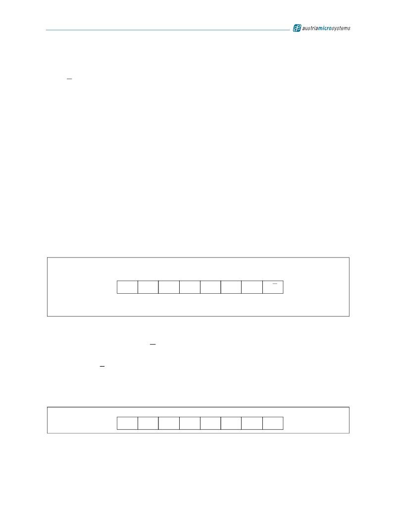
�I2C� Device� Address� Byte�
�The� address� byte� (see� Figure� 16)� is� the� first� byte� received� following� the� START� condition� from� the� master� device.�
�Figure� 16.� I2C� Device� Address� Byte�
�MSB�
�6�
�5�
�4�
�3�
�2�
�1�
�LSB�
�address:�
�0�
�1�
�1�
�1�
�0�
�AD1�
�AD0�
�R/W�
�-� The� bit� 1� and� bit� 2� of� the� address� byte� are� the� device� select� pins� AD0� and� AD1,� which� must� be� set� to� V� DD� or� to�
�GND.� A� maximum� of� four� devices� with� the� same� pre-set� code� can� therefore� be� connected� on� the� same� bus� at�
�one� time.�
�-� The� last� bit� of� the� address� byte� (R/W)� define� the� operation� to� be� performed.� When� set� to� a� 1� a� read� operation� is�
�selected;� when� set� to� a� 0� a� write� operation� is� selected.�
�Following� the� START� condition,� the� AS1119� monitors� the� I2C� bus,� checking� the� device� type� identifier� being� transmitted.� Upon� receiving� the�
�address� code,� and� the� R/W� bit,� the� slave� device� outputs� an� acknowledge� signal� on� the� SDA� line.�
�Command� Byte�
�The� AS1119� operation,� (� see� Table� 15� on� page� 21� )� is� determined� by� a� command� byte� (see� Table� 17)� .�
�Figure� 17.� Command� Byte�
�MSB�
�A7�
�6�
�A6�
�5�
�A5�
�4�
�A4�
�3�
�A3�
�2�
�A2�
�1�
�A1�
�LSB�
�A0�
��Revision� 1.04�
�11� -� 30�
�相关PDF资料 |
PDF描述 |
|---|---|
| AS1302-BWLT | IC REG BST SWITCHD CAP 5V 8WLCSP |
| AS1310-BTDT-18 | IC REG BOOST 1.8V 60MA 8TDFN |
| AS1322A-BTTT | IC REG BOOST SYNC ADJ TSOT23-6 |
| AS1323-BTTT-30 | IC REG BST SYNC 3V 0.1A TSOT23-5 |
| AS1324-BTTT-18 | IC REG BUCK SYNC 1.8V TSOT23-5 |
相关代理商/技术参数 |
参数描述 |
|---|---|
| AS1119DB | 制造商:ams 功能描述: |
| AS1119-DB | 制造商:ams 功能描述:AS1119 Demo Board with LED clip-on |
| AS1119-WK_DK_ST | 功能描述:AS1119 18, Non-Isolated Output LED Driver Evaluation Board 制造商:ams 系列:- 零件状态:有效 电流 - 输出/通道:- 输出和类型:18,非隔离 电压 - 输出:- 特性:可调光 电压 - 输入:2.7 V ~ 5.5 V 所含物品:板 使用的 IC/零件:AS1119 标准包装:1 |
| AS1119-XXX-I-A1-D | 制造商:未知厂家 制造商全称:未知厂家 功能描述:Analog Filter |
| AS1119-XXX-I-A1-S | 制造商:未知厂家 制造商全称:未知厂家 功能描述:Analog Filter |
发布紧急采购,3分钟左右您将得到回复。