- 您现在的位置:买卖IC网 > PDF目录13804 > AS1326A-BTDT (ams)IC REG BST SYNC 3.3V/ADJ 10TDFN PDF资料下载
参数资料
| 型号: | AS1326A-BTDT |
| 厂商: | ams |
| 文件页数: | 10/19页 |
| 文件大小: | 0K |
| 描述: | IC REG BST SYNC 3.3V/ADJ 10TDFN |
| 设计资源: | Design Support Tool |
| 标准包装: | 6,000 |
| 类型: | 升压(升压) |
| 输出类型: | 两者兼有 |
| 输出数: | 1 |
| 输出电压: | 3.3V,2.5 V ~ 5 V |
| 输入电压: | 0.7 V ~ 5 V |
| 频率 - 开关: | 1MHz |
| 电流 - 输出: | 800mA |
| 同步整流器: | 是 |
| 工作温度: | -40°C ~ 85°C |
| 安装类型: | 表面贴装 |
| 封装/外壳: | 10-WFDFN 裸露焊盘 |
| 包装: | 带卷 (TR) |
| 供应商设备封装: | 10-TDFN(3x3) |
�� �
�
�AS1326�
�Datasheet� -� D� e� t� a� i� l� e� d� D� e� s� c� r� i� p� t� i� o� n�
�8� Detailed� Description�
�The� AS1326A/AS1326B� are� high-efficiency,� low-noise� DC-DC� boost� converters� suitable� as� power� supplies� for� portable�
�devices.� Both� devices� feature� integrated� boost� switching� regulator,� N-channel� power� MOSFET,� P-channel� synchro-�
�nous� rectifier,� precision� reference,� and� shutdown� control� circuitry� (see� Figure� 1� on� page� 1)� .�
�The� AS1326A/AS1326B� are� able� to� boost� a� 1-� to� 3-cell� battery� voltage� input� to� a� fixed� 3.3V� output,� or� adjustable� output�
�between� 2.5� and� 5.0V� (an� external� Schottky� diode� is� required� for� output� voltages� greater� than� 4V).�
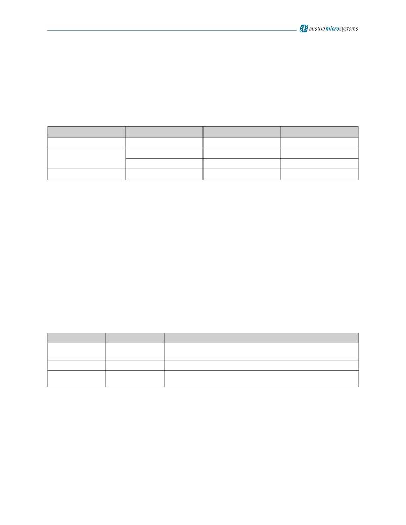
�Table� 5.� Typical� Output� Voltages� and� Currents�
�#� of� NiCd/NiMh� Cells�
�1�
�2�
�3�
�Input� Voltage� (V)�
�1.2�
�2.4�
�2.4�
�3.6�
�Output� Voltage� (V)�
�3.3�
�3.3�
�5.0�
�5.0�
�Output� Current� (mA)�
�335�
�800�
�450�
�800�
�The� devices� are� guaranteed� to� startup� with� an� input� voltage� as� low� as� 1.1V� and� remain� operational� down� to� an� input� of�
�as� little� as� 0.7V,� and� are� optimized� for� use� in� mobile� phones� and� other� RF� applications� which� have� low� noise� and� low�
�quiescent� current� (extended� battery� life)� requirements.�
�The� integrated� shutdown� circuitry� reduces� device� quiescent� current� down� to� 0.1μA.�
�Step-Up� Converter�
�During� boost� operation,� the� internal� N-channel� MOSFET� switch� turns� on� for� the� first� part� of� each� cycle,� allowing� current�
�to� ramp� up� in� the� inductor� and� store� energy� in� a� magnetic� field.� During� the� second� part� of� each� cycle,� the� MOSFET�
�turns� off� and� inductor� current� flows� through� the� synchronous� rectifier� to� the� output� filter� capacitor� and� the� load.� As� the�
�energy� stored� in� the� inductor� is� depleted,� the� current� ramps� down� and� the� synchronous� rectifier� turns� off.�
�At� light� loads,� the� device� operates� at� fixed-frequency� or� only� as� needed� to� maintain� regulation,� depending� on� the� set-�
��Operational� Modes�
�The� AS1326A/AS1326B� are� capable� of� operating� in� 3� different� modes� (see� Table� 6)� as� controlled� by� pin� CLK/SEL� (see�
��Table� 6.� Operational� Modes�
�CLK/SEL� Setting�
�0�
�1�
�External� 500kHz� to�
�1.2MHz� clock�
�Operational� Mode�
�Normal�
�Forced� PWM�
�Synchronized� PWM�
�Description�
�High-efficiency� at� all� loads;� Fixed-frequency� (1MHz)� at� heavy� and�
�medium� loads.�
�Fixed-frequency� (1MHz),� low-noise� at� all� loads.� V� IN� ≤� 0.75xV� OUT�
�Fixed-frequency,� low-noise� at� all� loads.� V� IN� ≤� 0.75xV� OUT�
�Normal� Operation�
�When� CLK/SEL� is� pulled� low,� the� devices� are� in� normal� operating� mode.� In� normal� mode� the� devices� operate� in� PWM�
�when� driving� medium-to-heavy� loads,� and� automatically� switches� to� automatic� powersave� mode� if� the� load� requires�
�less� power.� The� use� of� automatic� powersave� mode� will� boost� the� efficiency� futhermore� at� light-load� conditions.�
�Forced-PWM� Operation�
�Pulling� CLK/SEL� high,� selects� the� low-noise� PWM-only� mode.� During� forced-PWM� operation,� the� devices� switch� at� a�
�constant� frequency� (1MHz)� and� modulates� the� MOSFET� switch� pulse� width� to� control� the� power� transferred� per� cycle�
�to� regulate� the� output� voltage.� Switching� harmonics� generated� by� fixed-frequency� operation� are� consistent� and� can� be�
�filtered.� See� the� Noise� Spectrum� plot� in� the� Typical� Operating� Characteristics� (see� Figure� 14� on� page� 7)� .�
�www.austriamicrosystems.com�
�Revision� 1.05�
�9� -� 18�
�相关PDF资料 |
PDF描述 |
|---|---|
| SC3DF-100 | INDUCTOR SMD 10UH 0.63A 100KHZ |
| 160YXF12KEFCT78X11.5 | CAP ALUM 12UF 160V 20% RADIAL |
| 160YXF12KEFCTA8X11.5 | CAP ALUM 12UF 160V 20% RADIAL |
| 160YXF12KEFC8X11.5 | CAP ALUM 12UF 160V 20% RADIAL |
| SC3316F-681 | INDUCTOR SMD 680UH 0.4A 100KHZ |
相关代理商/技术参数 |
参数描述 |
|---|---|
| AS1326A-BTDT-1K | 功能描述:IC REG BST SYNC 3.3V/ADJ 10-TDFN RoHS:是 类别:集成电路 (IC) >> PMIC - 稳压器 - DC DC 开关稳压器 系列:- 标准包装:50 系列:- 类型:升压(升压) 输出类型:可调式 输出数:1 输出电压:5 V ~ 25 V 输入电压:2.3 V ~ 5.5 V PWM 型:电流模式 频率 - 开关:600kHz,1.2MHz 电流 - 输出:1A 同步整流器:无 工作温度:-40°C ~ 85°C 安装类型:表面贴装 封装/外壳:8-TSSOP,8-MSOP(0.118",3.00mm 宽) 包装:管件 供应商设备封装:8-MSOP |
| AS1326A-BTDU | 制造商:ams 功能描述:DC-DC Step Up, Fixed, Sync, 0.7 to 5.0V input, 3.3, 2.5 to 5.0V (650mA) Output, 96% Efficiency, 1200 kHz fmax, TDFN-10, Synchronizes to External Clock, Tray |
| AS1326A-TD_EK_ST | 功能描述:AS1326 - DC/DC, Step Up 1, Non-Isolated Outputs Evaluation Board 制造商:ams 系列:- 零件状态:有效 主要用途:DC/DC,步升 输出和类型:1,非隔离 功率 - 输出:- 电压 - 输出:3.3V 电流 - 输出:800mA 电压 - 输入:0.7 V ~ 5 V 稳压器拓扑:升压 频率 - 开关:1MHz 板类型:完全填充 所含物品:板 使用的 IC/零件:AS1326 标准包装:1 |
| AS1326B | 制造商:AMSCO 制造商全称:austriamicrosystems AG 功能描述:High Current, 0.8A DC-DC Step-Up Converters |
| AS1326B-BTDR | 功能描述:IC REG BST SYNC 3.3V/ADJ 10TDFN RoHS:是 类别:集成电路 (IC) >> PMIC - 稳压器 - DC DC 开关稳压器 系列:- 产品培训模块:MIC23xxx HyperLight Load™ Regulators 标准包装:5,000 系列:HyperLight Load® 类型:降压(降压) 输出类型:固定 输出数:1 输出电压:1.8V 输入电压:2.7 V ~ 5.5 V PWM 型:混合物 频率 - 开关:4MHz 电流 - 输出:2A 同步整流器:是 工作温度:-40°C ~ 125°C 安装类型:表面贴装 封装/外壳:8-VFDFN 裸露焊盘,8-MLF? 包装:带卷 (TR) 供应商设备封装:8-MLF?(2x2) 产品目录页面:1094 (CN2011-ZH PDF) 其它名称:576-3303-2 |
发布紧急采购,3分钟左右您将得到回复。