- 您现在的位置:买卖IC网 > PDF目录11203 > AS1751S-T (ams)IC SWITCH QUAD SPST 14-TSSOP PDF资料下载
参数资料
| 型号: | AS1751S-T |
| 厂商: | ams |
| 文件页数: | 2/17页 |
| 文件大小: | 0K |
| 描述: | IC SWITCH QUAD SPST 14-TSSOP |
| 标准包装: | 2,500 |
| 功能: | 开关 |
| 电路: | 4 x SPST - NO |
| 导通状态电阻: | 900 毫欧 |
| 电压电源: | 单电源 |
| 电压 - 电源,单路/双路(±): | 1.6 V ~ 3.6 V |
| 电流 - 电源: | 100nA |
| 工作温度: | -40°C ~ 85°C |
| 安装类型: | 表面贴装 |
| 封装/外壳: | 14-TSSOP(0.173",4.40mm 宽) |
| 供应商设备封装: | 14-TSSOP |
| 包装: | 带卷 (TR) |
www.austriamicrosystems.com
Revision 1.41
9 - 16
AS1751/AS1752/AS1753
Data Sheet - Ap p lica tio n In fo r m a tio n
9 Application Information
Power Supply Sequencing
Proper power-supply sequencing is critical for proper switch operation. The power supplies should be started up in the
following sequence:
1. V+
2. NOx, NCx, COMx
Note: Do not exceed the absolute maximum ratings (see page 2).
Overvoltage Protection
ON-resistance increases slightly at lower supply voltages.
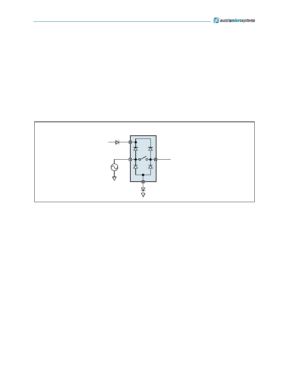
Figure 12. Overvoltage Protection using 2 External Blocking Diodes
Adding diode D2 to the circuit shown in Figure 12 causes the logic threshold to be shifted relative to GND. Diodes D1
and D2 also protect against overvoltage conditions.
For example, in the circuit shown in Figure 12, if the supply voltage goes below the absolute maximum rating, and if a
fault voltage up to the absolute maximum rating is applied to an analog signal pin, no damage will result.
Power Supply Bypass
Power supply connections to the devices must maintain a low impedance to ground. This can be done using a bypass
capacitor, which will also improve noise margin and prevent switching noise propagation from the V+ supply to other
components.
A 0.1F bypass capacitor, connected from V+ to GND (see Figure 18 on page 11), is adequate for most applications.
Logic Inputs
Driving INx Rail-to-Rail will help minimize power consumption.
Layout Considerations
High-speed switches require proper layout and design procedures for optimum performance.
!
Short, wide traces should be used to reduce stray inductance and capacitance.
!
Bypass capacitors should be as close to the device as possible.
!
Large ground planes should be used wherever possible.
AS1751/AS1752/AS1753
GND
VGEN
COMx
D2
D1
V+
NOx
AG
Technical
content
still
valid
相关PDF资料 |
PDF描述 |
|---|---|
| VE-B41-IX | CONVERTER MOD DC/DC 12V 75W |
| VE-B41-IW | CONVERTER MOD DC/DC 12V 100W |
| VI-JTL-IW | CONVERTER MOD DC/DC 28V 100W |
| VI-JTJ-IW | CONVERTER MOD DC/DC 36V 100W |
| VI-JTH-IW | CONVERTER MOD DC/DC 52V 100W |
相关代理商/技术参数 |
参数描述 |
|---|---|
| AS1751V | 制造商:AMSCO 制造商全称:austriamicrosystems AG 功能描述:High-Speed, Low-Voltage, Single-Supply, 0.9, Quad SPST Analog Switches |
| AS1751V-T | 功能描述:IC SWITCH QUAD SPST 16TQFN RoHS:是 类别:集成电路 (IC) >> 接口 - 模拟开关,多路复用器,多路分解器 系列:- 其它有关文件:STG4159 View All Specifications 标准包装:5,000 系列:- 功能:开关 电路:1 x SPDT 导通状态电阻:300 毫欧 电压电源:双电源 电压 - 电源,单路/双路(±):±1.65 V ~ 4.8 V 电流 - 电源:50nA 工作温度:-40°C ~ 85°C 安装类型:表面贴装 封装/外壳:7-WFBGA,FCBGA 供应商设备封装:7-覆晶 包装:带卷 (TR) |
| AS1752 | 制造商:AMSCO 制造商全称:austriamicrosystems AG 功能描述:High-Speed, Low-Voltage, Single-Supply, 0.9ヘ, Quad SPST Analog Switches |
| AS1752S | 功能描述:模拟开关 IC RoHS:否 制造商:Texas Instruments 开关数量:2 开关配置:SPDT 开启电阻(最大值):0.1 Ohms 切换电压(最大): 开启时间(最大值): 关闭时间(最大值): 工作电源电压:2.7 V to 4.5 V 最大工作温度:+ 85 C 安装风格:SMD/SMT 封装 / 箱体:DSBGA-16 |
| AS1752S-T | 功能描述:IC SWITCH QUAD SPST 14-TSSOP RoHS:是 类别:集成电路 (IC) >> 接口 - 模拟开关,多路复用器,多路分解器 系列:- 其它有关文件:STG4159 View All Specifications 标准包装:5,000 系列:- 功能:开关 电路:1 x SPDT 导通状态电阻:300 毫欧 电压电源:双电源 电压 - 电源,单路/双路(±):±1.65 V ~ 4.8 V 电流 - 电源:50nA 工作温度:-40°C ~ 85°C 安装类型:表面贴装 封装/外壳:7-WFBGA,FCBGA 供应商设备封装:7-覆晶 包装:带卷 (TR) |
发布紧急采购,3分钟左右您将得到回复。