参数资料
| 型号: | AS3510 |
| 厂商: | ams |
| 文件页数: | 20/20页 |
| 文件大小: | 0K |
| 描述: | IC CODEC AFE ANALOG 49-CABGA |
| 标准包装: | 476 |
| 类型: | 音频编解码器 |
| 应用: | 便携式音频,电话 |
| 安装类型: | 表面贴装 |
| 封装/外壳: | 49-WFBGA |
| 供应商设备封装: | 49-CSBGA(7x7) |
| 包装: | 托盘 |
Product Brief AS3510
Rev. 1v2, June 2004
CONFIDENTIAL
Page 8 of 19
Supply Regulator
Block Description
This block can be used to provide three regulated supply
voltages for the
-
on_chip digital section
-
on_chip analog section
-
external circuit (uP, DSP…)
from the battery supply BVDD which is directly used by the
power_amplifier.
The LDO1 and LDO2 do have the capability to drive 50mA
with a voltage drop of <=50mV (1Ohm). Since the nominal
output voltage for these LDOs is 2.9V (+/-50mV), a
regulation can be done with BVDD as low as 3.0V.
The LDO3 is used to generate a supply voltage PVDD for
the peripheral cells and external digital circuits, which are
controlling the inputs of the AS3510. The drive capability is
≥200mA with a BVDD≥3V.
The maximum output currents for these LDOs can be
calculated using the following equation:
Ohm
mV
Vout
BVDD
I
1
50
)
(
max
+
=
Vout is 2.9V for LDO1 and LDO2. The output Voltage for
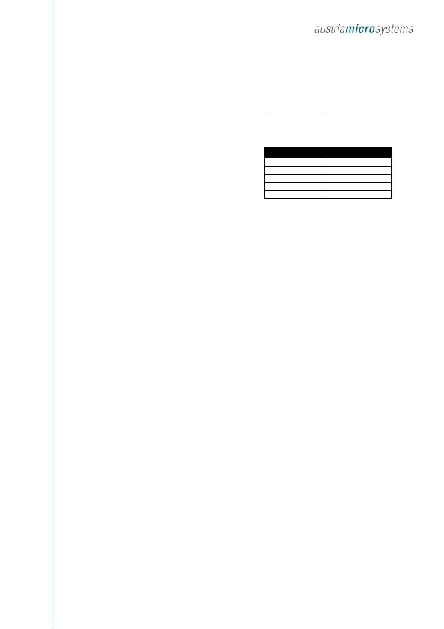
LDO3 can be programmed via the PLDO3 pin.
PLD3 pin
QLDO3 voltage
VSS
2.25V
150k to VSS
2.0V
open
2.5
150k to DVDD
1.5
DVDD
1.75
Table 10
LDO3 Programming
There are two pads at each LDO, one is the LDO output pad
and the second is the corresponding chip supply pad, which
are bonded to the same pin (LDO1 only), and have external
blocking caps (Cblock with low ESR).
If supply should not be generated from the on_chip LDOs,
these blocks can be disabled with control pin PowerUP.
AVDD, DVDD and PVDD can then be forced from external
regulators.
ams
AG
Technical
content
still
valid
相关PDF资料 |
PDF描述 |
|---|---|
| AS3515-T | IC CODEC AFE AUDIO STER 64-CABGA |
| AS3515 | IC CODEC AFE AUDIO STER 64-CABGA |
| AS3517-T | IC CODEC AFE AUDIO STER 81-CTBGA |
| AS3543-ECTP | IC CODEC AUDIO FRONT END 68CTBGA |
| ASM2I9940LG-32LT | IC CLK BUFFER 2:18 250MHZ 32LQFP |
相关代理商/技术参数 |
参数描述 |
|---|---|
| AS3510018 | 制造商:AMETHERM 制造商全称:AMETHERM Circuit Protection Thermistors 功能描述:Resistance @ 25°c |
| AS3510-0212K | 制造商:AS PN'S 功能描述: |
| AS35100FLF | 制造商:TT Electronics / IRC 功能描述:AS35100FLF |
| AS35100HLF | 制造商:TT Electronics / IRC 功能描述:AS35100HLF |
| AS35100JLF | 制造商:TT Electronics / IRC 功能描述:AS35100JLF |
发布紧急采购,3分钟左右您将得到回复。