- 您现在的位置:买卖IC网 > Datasheet目录60 > AS5132-HSST-500 (ams)IC ENCODER ROTARY 20-SSOP Datasheet资料下载
参数资料
| 型号: | AS5132-HSST-500 |
| 厂商: | ams |
| 文件页数: | 13/27页 |
| 文件大小: | 522K |
| 描述: | IC ENCODER ROTARY 20-SSOP |
| 标准包装: | 1 |
| 传感范围: | 20mT ~ 80mT |
| 类型: | 旋转 |
| 电源电压: | 4.5 V ~ 5.5 V |
| 电流 - 电源: | 15mA |
| 输出类型: | 数字式,PWM,8.5 位串行 |
| 特点: | 可编程 |
| 工作温度: | -40°C ~ 150°C |
| 封装/外壳: | 20-SSOP(0.209",5.30mm 宽) |
| 供应商设备封装: | 20-SSOP |
| 包装: | 标准包装 |
| 其它名称: | AS5132-HSST-500DKR |
第1页第2页第3页第4页第5页第6页第7页第8页第9页第10页第11页第12页当前第13页第14页第15页第16页第17页第18页第19页第20页第21页第22页第23页第24页第25页第26页第27页
www.ams.com
Revision 1.4
13 - 27
AS5132
Datasheet - Detailed Description
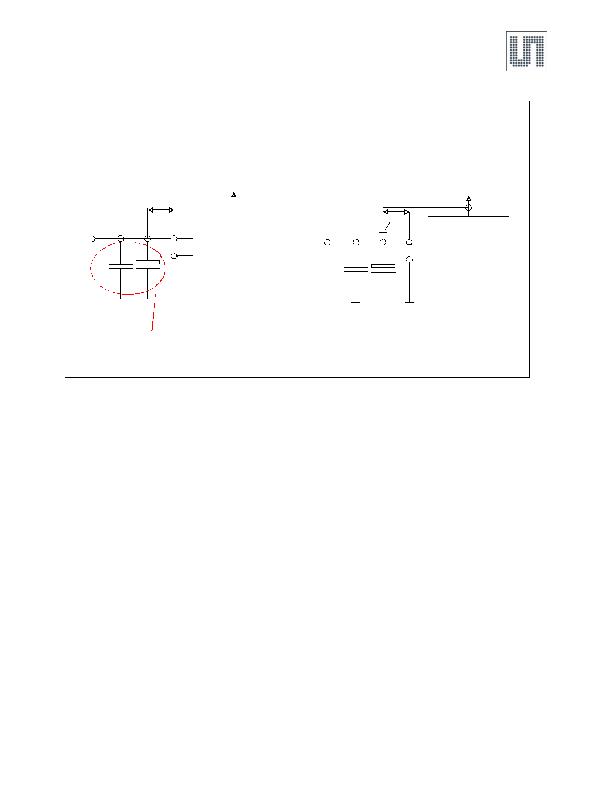
Figure 11. OTP Programming Connection
Note: The maximum capacitive load at PROG in normal operation should be less than 20pF. However, during programming the capacitors
C1+C2 are needed to buffer the programming voltage during current spikes, but they must be removed for normal operation. To
overcome this contradiction, the recommendation is to add a diode (4148 or similar) between PROG and VDD as shown in Figure 11
(special case setup), if the capacitors can not be removed at final assembly.
Due to D1, the capacitors C1+C2 are loaded with VDD-0.7V at startup, hence not influencing the readout of the internal OTP registers.
During programming the OTP, the diode ensures that no current is flowing from PROG (8V to 8.5V) to VDD (5V).
In the standard case (see Figure 11), the verification of a correct OTP readout must be done by analog readback. The special case
setup provides the analog readback of the OTP as well.
As long as the PROG pin is accessible it is recommended to use standard setup. In case the PROG pin is not accessible at final
assembly, the special setup is recommended.
7.1.3 Programming Verification
After programming, the programmed OTP bits must be verified using the following methods:
Digital Read Out (Mandatory): After sending a READ OTP command, the readback information must be the same as programmed
information. Otherwise, it indicates that the programming was not performed correctly.
Note: Either
Digital Verification
or
Analog Verification
must be carried out in addition to the
Digital Read Out
.
Digital Verification: Checking the EZ ERR bit (0 = OK, 1 = error)
i) At room temperature
ii) Right after the programming
Analog Verification: By switching into Extended Mode and sending a READ ANA command, the pin PROG becomes an output sending an
analog voltage with each clock representing a sequence of the bits in the OTP register (starting with D61). A voltage of <500mV indicates a
correctly programmed bit (
1
) while a voltage level between 2V and 3.5V indicates a correctly unprogrammed bit (
0
). Any voltage level in
between indicates incorrect programming.
VDD
V
SUPPLY
PROG
GND
C1
C2
100nF
10礔
V
zapp
V
prog
PROM Cell
Maximum
parasitic cable
inductance
L<50nH
Standard Case
VDD
V
SUPPLY
PROG
GND
C1
C2
100nF
10礔
V
zapp
V
prog
PROM Cell
L<50nH
Special Case
Remove for normal operation
相关PDF资料 |
PDF描述 |
|---|---|
| AS5134-ZSST-500 | IC ENCODER RPTARY 20-SSOP |
| AS5140H-ASST | IC ENCODER ROTARY 10BIT 16-SSOP |
| AS5145B-HSST-500 | IC ENCODER ROTARY MAGN 16-SSOP |
| AS5510-DWLT | IC ENCODER MAGNETIC LIN 6-WLCSP |
| ATS137-PL-B-B | IC HALL SENSOR SGL 25MA SIP-3L |
相关代理商/技术参数 |
参数描述 |
|---|---|
| AS5132-SS_EK_AB | 功能描述:AS5132 - Magnetic, Rotary Position Sensor Evaluation Board 制造商:ams 系列:- 零件状态:有效 传感器类型:磁性,旋转位置 感应范围:360° 接口:串行 灵敏度:- 电压 - 电源:4.5 V ~ 5.5 V 嵌入式:否 所含物品:板 使用的 IC/零件:AS5132 标准包装:1 |
| AS5132-SS_EK_DB | 功能描述:AS5132 - Magnetic, Rotary Position Sensor Evaluation Board 制造商:ams 系列:- 零件状态:有效 传感器类型:磁性,旋转位置 感应范围:360° 接口:串行 灵敏度:- 电压 - 电源:4.5 V ~ 5.5 V 嵌入式:- 所含物品:板 使用的 IC/零件:AS5132 标准包装:1 |
| AS5132-SS_EK_PB | 功能描述:AS5132 - ZIF Socket 制造商:ams 系列:- 零件状态:有效 模块/板类型:ZIF 插口 配套使用产品/相关产品:AS5132 标准包装:1 |
| AS51331FLF | 制造商:TT Electronics / IRC 功能描述:AS51331FLF |
| AS51331JLF | 制造商:TT Electronics / IRC 功能描述:AS51331JLF |
发布紧急采购,3分钟左右您将得到回复。