- 您现在的位置:买卖IC网 > PDF目录381325 > AS7C256L-35TC (ALLIANCE SEMICONDUCTOR CORP) High Performance 32Kx8 CMOS SRAM PDF资料下载
参数资料
| 型号: | AS7C256L-35TC |
| 厂商: | ALLIANCE SEMICONDUCTOR CORP |
| 元件分类: | DRAM |
| 英文描述: | High Performance 32Kx8 CMOS SRAM |
| 中文描述: | 32K X 8 STANDARD SRAM, 35 ns, PDSO28 |
| 封装: | 8 X 13.40 MM, TSOP1-28 |
| 文件页数: | 6/8页 |
| 文件大小: | 125K |
| 代理商: | AS7C256L-35TC |
AS7C256
AS7C256L
6
1. During V
CC
power-up, a pull-up resistor to V
CC
on CE is required to meet I
SB
specification.
2. This parameter is sampled and not 100% tested.
3. For test conditions, see
AC Test Conditions
, Figures A, B, C.
4. t
CLZ
and t
CHZ
are specified with CL = 5pF as in Figure C. Transition is measured
±
500mV from steady-state voltage.
5. This parameter is guaranteed but not tested.
6. WE is HIGH for read cycle.
7. CE and OE are LOW for read cycle.
8. Address valid prior to or coincident with CE transition LOW.
9. All read cycle timings are referenced from the last valid address to the first transitioning address.
10. CE or WE must be HIGH during address transitions.
11. All write cycle timings are referenced from the last valid address to the first transitioning address.
Parameter
Symbol
Test Conditions
Min
Max
Unit
V
CC
for Data Retention
Data Retention Current
V
DR
I
CCDR
t
CDR
t
R
|
I
LI
|
V
CC
= 2.0V
CE
≥
V
CC
–0.2V
V
in
≥
V
–0.2V
or
V
in
≤
0.2V
2.0
–
V
μ
A
–
150
Chip Enable to Data Retention Time
0
–
ns
Operation Recovery Time
t
RC
–
–
ns
μ
A
Input Leakage Current
1
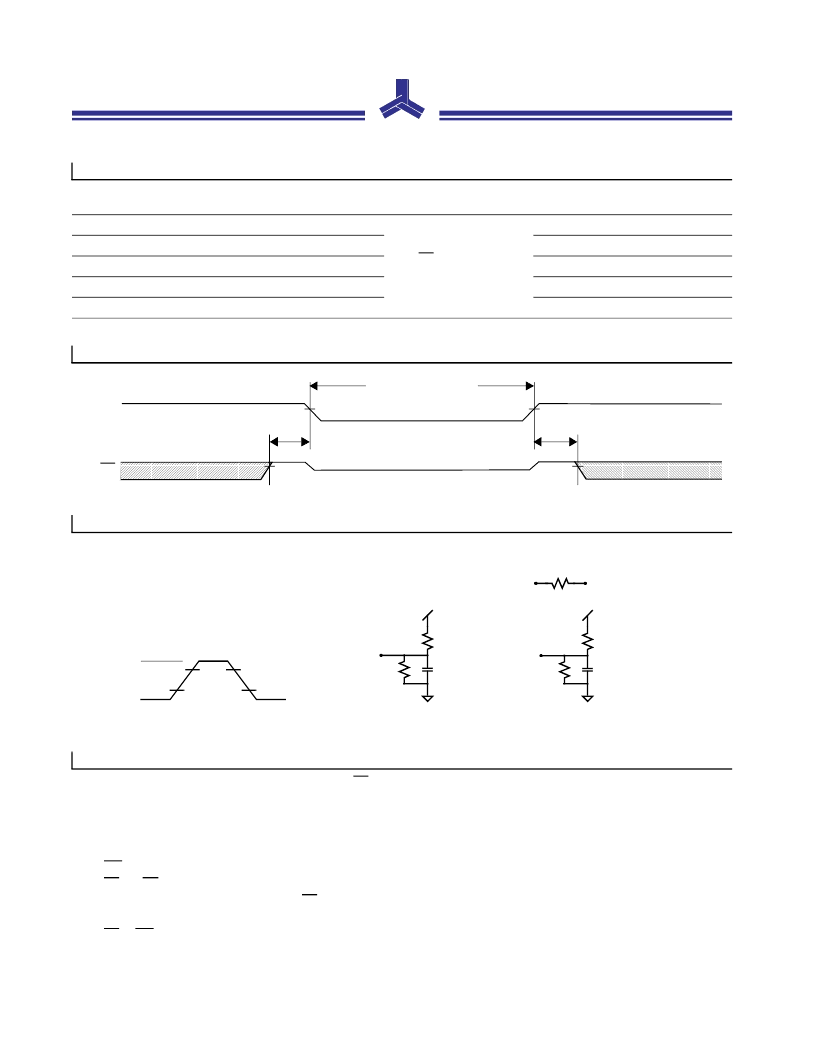
DATA RETENTION CHARACTERISTICS
(L Version Only)
DATA RETENTION WAVEFORM
(L Version Only)
AAAA
AAAA
AAAA
AAAA
AAAA
AAAA
AAAA
AAAA
AAAA
AAAA
AAAA
AAAA
AAAA
AAAA
AAAA
AAAA
AAAA
AAAA
AAAA
AAAA
AAAA
AS7C256-07
AAAA
AAAA
AAAA
AAAA
AAAA
AAAA
AAAA
AAA
AAA
AAA
AAA
AAAA
AAAA
AAAA
AAAA
AAAA
AAAA
AAAA
AAAA
AAAA
AAAA
AAAA
AAAA
AAAA
AAAA
AAAA
AAAA
AAAA
AAAA
AAAA
AAAA
AAAA
AAAA
AAAA
AAAA
AAAA
AAAA
AAAA
AAAA
AAA
AAA
AAA
AAA
V
CC
CE
t
R
t
CDR
Data retention mode
4.5V
4.5V
V
DR
≥
2.0V
V
IH
V
IH
V
DR
AC TEST CONDITIONS
255
– Output load: see Figure B,
except for t
CLZ
and t
CHZ
see Figure C.
– Input pulse level: GND to 3.0V. See Figure A.
– Input rise and fall times: 5 ns. See Figure A.
– Input and output timing reference levels: 1.5V.
5 pF*
480
D
out
GND
+5V
168
Thevenin Equivalent:
D
out
+1.728V
Figure C: Output Load for t
CLZ
, t
CHZ
AS7C256-10
255
30 pF*
480
D
out
GND
+5V
Figure B: Output Load
AS7C256-09
*including scope
and jig capacitance
10%
90%
10%
90%
GND
+3.0V
Figure A: Input Waveform
AS7C256-08
NOTES
相关PDF资料 |
PDF描述 |
|---|---|
| AS7C256L-12JC | High Performance 32Kx8 CMOS SRAM |
| AS7C256L-10JC | High Performance 32Kx8 CMOS SRAM |
| AS7C256L-10PC | High Performance 32Kx8 CMOS SRAM |
| AS7C256L-10SC | High Performance 32Kx8 CMOS SRAM |
| AS7C256L-10TC | High Performance 32Kx8 CMOS SRAM |
相关代理商/技术参数 |
参数描述 |
|---|---|
| AS7C256L-55PC | 制造商:未知厂家 制造商全称:未知厂家 功能描述:x8 SRAM |
| AS7C256L-55SC | 制造商:未知厂家 制造商全称:未知厂家 功能描述:x8 SRAM |
| AS7C256L-55TC | 制造商:未知厂家 制造商全称:未知厂家 功能描述:x8 SRAM |
| AS7C256L-70PC | 制造商:未知厂家 制造商全称:未知厂家 功能描述:x8 SRAM |
| AS7C256L-70SC | 制造商:未知厂家 制造商全称:未知厂家 功能描述:x8 SRAM |
发布紧急采购,3分钟左右您将得到回复。