- 您现在的位置:买卖IC网 > PDF目录362465 > AT10-0019TR PIN Diode Based Variable Attenuator, 50 - 1000 MHz PDF资料下载
参数资料
| 型号: | AT10-0019TR |
| 英文描述: | PIN Diode Based Variable Attenuator, 50 - 1000 MHz |
| 中文描述: | 基于PIN二极管可变衰减器,50 - 1000兆赫 |
| 文件页数: | 1/2页 |
| 文件大小: | 220K |
| 代理商: | AT10-0019TR |
PIN Diode Based V ariable
Attenuator, 50 - 1000 MHz
A
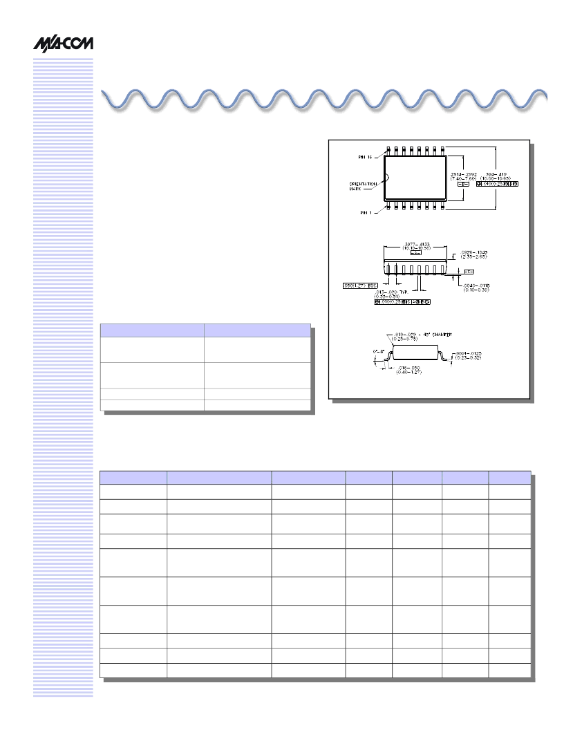
SOW-16
V 5.00
Electrical Specifications
2
: T
A
= 25°C
Features
I
High Dynamic Range: 42dB Typical
I
Flat Attenuation vs. Frequency
I
High P1dB Compression
I
Operates on a Single +5V Supply:
I
SOW-16, Wide Body Package
I
50 Ohm Nominal Impedance
Description
M/A-COM's AT10-0019 is a Voltage Controlled PIN diode
based
π
attenuator packaged in a low cost, 16 lead wide
body plastic SMT package. The PIN diode design makes
this part well suited for applications where low distortion or
high linear operating power levels are required. These
attenuators are ideal for gain control in multi-channel
digital communications systems.
Package outline conforms to JEDEC standard MS-013AA.
Parameter
Test Conditions
Frequency
Units
Min
Typical
Max
Insertion Loss
Vcont.: +10 V
50 - 1000 MHz
dB
—
2.4
2.8
Dynamic Range
Vcont.: 0 V
50 - 1000 MHz
dB
33
42
—
Attenuation
Flatness
VSWR
Attenuation: 0 to 20 dB
Attenuation: 20 to 30 dB
Vcont.: 0 - 10V
50 - 1000 MHz
50 - 1000 MHz
50 - 1000 MHz
dB
dB
Ratio
—
—
—
1.0
1.5
1.7:1
1.5
2.0
2.1:1
Trise, Tfall
Ton, Toff
Transients
1 dB
Compression
10%/90%, 90%/10%
50% Cntl to 90%/10% RF
In-band
Vcont.: 0 - 10V
—
μS
μS
mV
dBm
dBm
dBm
dBm
dBm
—
—
—
10
17
21
24
34
10
15
150
13
20
24
27
37
20
25
250
—
—
—
—
—
100 MHz
500 MHz
1000 MHz
100 MHz
1000 MHz
Input IP
3
Vcont.: 0 - 10V
Two-tone inputs up to +10
dBm
—
V
CC
—
V
+4.75
+5.0
+5.25
I
CC
V
CC
= 5.25 V
DC
mA
—
2
2.5
Control Current
—
DC
mA
—
2.7
3.5
2. Unit requires external .01 μF DC Blocks on RF lines.
Parameter
Max. Input Power
50 - 500 MHz
500 - 1000 MHz
Voltages
Absolute Maximum
+24 dBm
+30 dBm
-1 V to +7.0 V
-1 V to +15 V
-40°C to +85°C
-65°C to +125°C
V
Control Voltage
Operating Temperature
Storage Temperature
Absolute Maximum Ratings
1
1. Operation of this device above any one of these parameters
may cause permanent damage.
相关PDF资料 |
PDF描述 |
|---|---|
| AT104 | Thick Film Chip Resistor - RMC 1/2 374K 1% R |
| AT107 | Digital Attenuator, 31.5 dB, 6-Bit, TTL Driver DC2 GHz |
| AT118PIN | Industrial Control IC |
| AT118TR | Industrial Control IC |
| AT1201 | AT1201 - Low-Noise 2.7V/2.8V/3.0V/3.3V/5.0V 150mA LDO Regulator |
相关代理商/技术参数 |
参数描述 |
|---|---|
| AT10-0019-TR | 制造商:未知厂家 制造商全称:未知厂家 功能描述:PIN Diode based Variable Attenuator 501000 MHz |
| AT1000-20 | 制造商:Amphenol Corporation 功能描述:AT1000-20 - Bulk |
| AT-1001 | 制造商:HRS 制造商全称:HRS 功能描述:High Power Fixed Attenuators (Radiator built-in) |
| AT-1001(40) | 功能描述:衰减器 -互连 RoHS:否 制造商:Pomona Electronics 最大衰减: 容差: 频率范围:DC to 500 MHz 阻抗:50 Ohms 功率额定值:2 W 端接类型:Crimp 连接器类型:BNC Male / Female 工作温度范围:0 C to + 102 C |
| AT10013A | 制造商:Sliger Designs, Inc. 功能描述:RACK EAR, SILVER, FOR AT1101D-BK CHASSIS - Bulk |
发布紧急采购,3分钟左右您将得到回复。