- 您现在的位置:买卖IC网 > PDF目录19914 > AT17F080-30CU (Atmel)IC FLASH CONFIG 8M 8LAP PDF资料下载
参数资料
| 型号: | AT17F080-30CU |
| 厂商: | Atmel |
| 文件页数: | 16/19页 |
| 文件大小: | 0K |
| 描述: | IC FLASH CONFIG 8M 8LAP |
| 标准包装: | 100 |
| 可编程类型: | 闪存 |
| 存储容量: | 8Mb |
| 电源电压: | 2.97 V ~ 3.63 V |
| 工作温度: | -40°C ~ 85°C |
| 封装/外壳: | 8-TDFN |
| 供应商设备封装: | 8-LAP(6x6) |
| 包装: | 管件 |
| 产品目录页面: | 609 (CN2011-ZH PDF) |
| 配用: | ATDH2225-ND - CABLE ISP FOR AT17 ATDH2200E-ND - CONFIGURATOR PROGRAM BOARD KIT |
6
3039K–CNFG–2/08
AT17F040/080
5.4
PAGESEL[1:0](2)
Page select inputs. Used to determine which of the 4 memory pages are targeted during a serial
configuration download. The address space for each of the pages is shown in Table 5-2. When
SER_EN is Low (ISP mode) these pins have no effect.
5.5
RESET/OE(1)
Output Enable (active High) and RESET (active Low) when SER_EN is High. A Low level on
RESET/OE resets both the address and bit counters. A High level (with CE Low) enables the
data output driver.
5.6
CE(1)
Chip Enable input (active Low). A Low level (with OE High) allows CLK to increment the address
counter and enables the data output driver. A High level on CE disables both the address and bit
counters and forces the device into a low-power standby mode. Note that this pin will not
enable/disable the device in the 2-wire Serial Programming mode (SER_EN Low).
5.7
GND
Ground pin. A 0.2 F decoupling capacitor between V
CC and GND is recommended.
5.8
CEO
Chip Enable Output (when SER_EN is High). This output goes Low when the internal address
counter has reached its maximum value. If the PAGE_EN input is set High, the maximum value
is the highest address in the selected partition. The PAGESEL[1:0] inputs are used to make the
4 partition selections. If the PAGE_EN input is set Low, the device is not partitioned and the
address maximum value is the highest address in the device, see Table 5-2 on page 6. In a
daisy chain of AT17F Series devices, the CEO pin of one device must be connected to the CE
input of the next device in the chain. It will stay Low as long as CE is Low and OE is High. It will
then follow CE until OE goes Low; thereafter, CEO will stay High until the entire EEPROM is
read again.
Notes:
1. This pin has an internal 20 k
pull-up resistor.
2. This pin has an internal 30 k
pull-down resistor.
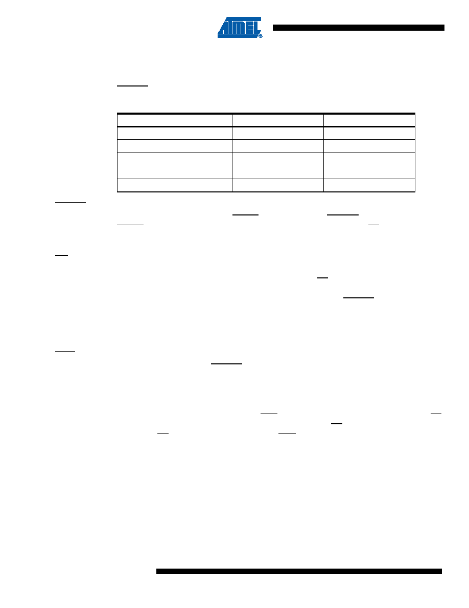
Table 5-2.
Address Space
Paging Decodes
AT17F040 (4 Mbits)
AT17F080 (8 Mbits)
PAGESEL = 00, PAGE_EN = 1
00000 – 0FFFFh
00000 – 1FFFFh
PAGESEL = 01, PAGE_EN = 1
10000 – 1FFFFh
20000 – 3FFFFh
PAGESEL = 10, PAGE_EN = 1
20000 – 2FFFFh
40000 – 5FFFFh
PAGESEL = 11, PAGE_EN = 1
30000 – 3FFFFh
60000 – 7FFFFh
PAGESEL = XX, PAGE_EN = 0
00000 – 3FFFFh
00000 – 7FFFFh
相关PDF资料 |
PDF描述 |
|---|---|
| LTC4308CDD#PBF | IC BUS BUFFER LV 8-DFN |
| VE-JNL-CY-B1 | CONVERTER MOD DC/DC 28V 50W |
| HSM36DSEH | CONN EDGECARD 72POS .156 EYELET |
| AT18F002-30XU | IC FLASH CONFIG 2MBIT 20-TSSOP |
| LTC4307CDD-1#PBF | IC BUFFER 2-WIRE BUS 8-DFN |
相关代理商/技术参数 |
参数描述 |
|---|---|
| AT17F080-30JC | 功能描述:FPGA-配置存储器 Serial Flash RoHS:否 制造商:Altera Corporation 存储类型:Flash 存储容量:1.6 Mbit 工作频率:10 MHz 电源电压-最大:5.25 V 电源电压-最小:3 V 电源电流:50 uA 最大工作温度:+ 85 C 最小工作温度:- 40 C 安装风格:SMD/SMT 封装 / 箱体:PLCC-20 |
| AT17F080-30JI | 功能描述:FPGA-配置存储器 Serial Flash RoHS:否 制造商:Altera Corporation 存储类型:Flash 存储容量:1.6 Mbit 工作频率:10 MHz 电源电压-最大:5.25 V 电源电压-最小:3 V 电源电流:50 uA 最大工作温度:+ 85 C 最小工作温度:- 40 C 安装风格:SMD/SMT 封装 / 箱体:PLCC-20 |
| AT17F080-30JU | 功能描述:FPGA-配置存储器 FPGA SERIAL CONFIG 30MHZ IND TEMP GREEN RoHS:否 制造商:Altera Corporation 存储类型:Flash 存储容量:1.6 Mbit 工作频率:10 MHz 电源电压-最大:5.25 V 电源电压-最小:3 V 电源电流:50 uA 最大工作温度:+ 85 C 最小工作温度:- 40 C 安装风格:SMD/SMT 封装 / 箱体:PLCC-20 |
| AT17F080-30JU SL383 | 制造商:Atmel Corporation 功能描述:FPGA SERIAL CONFIG FLASH, 8M - 30MHZ, 20 PLCC, IND TEMP, GRE - Tape and Reel |
| AT17F080-30TQC | 功能描述:FPGA-配置存储器 FPGA SERIAL CONFIG 30MHZ 3.3V COM TEMP RoHS:否 制造商:Altera Corporation 存储类型:Flash 存储容量:1.6 Mbit 工作频率:10 MHz 电源电压-最大:5.25 V 电源电压-最小:3 V 电源电流:50 uA 最大工作温度:+ 85 C 最小工作温度:- 40 C 安装风格:SMD/SMT 封装 / 箱体:PLCC-20 |
发布紧急采购,3分钟左右您将得到回复。