- 您现在的位置:买卖IC网 > PDF目录362467 > AT22LV10L-35GI UV-Erasable/OTP PLD PDF资料下载
参数资料
| 型号: | AT22LV10L-35GI |
| 英文描述: | UV-Erasable/OTP PLD |
| 中文描述: | UV-Erasable/OTP可编程逻辑器件 |
| 文件页数: | 7/12页 |
| 文件大小: | 410K |
| 代理商: | AT22LV10L-35GI |
AT22LV10(L)
7
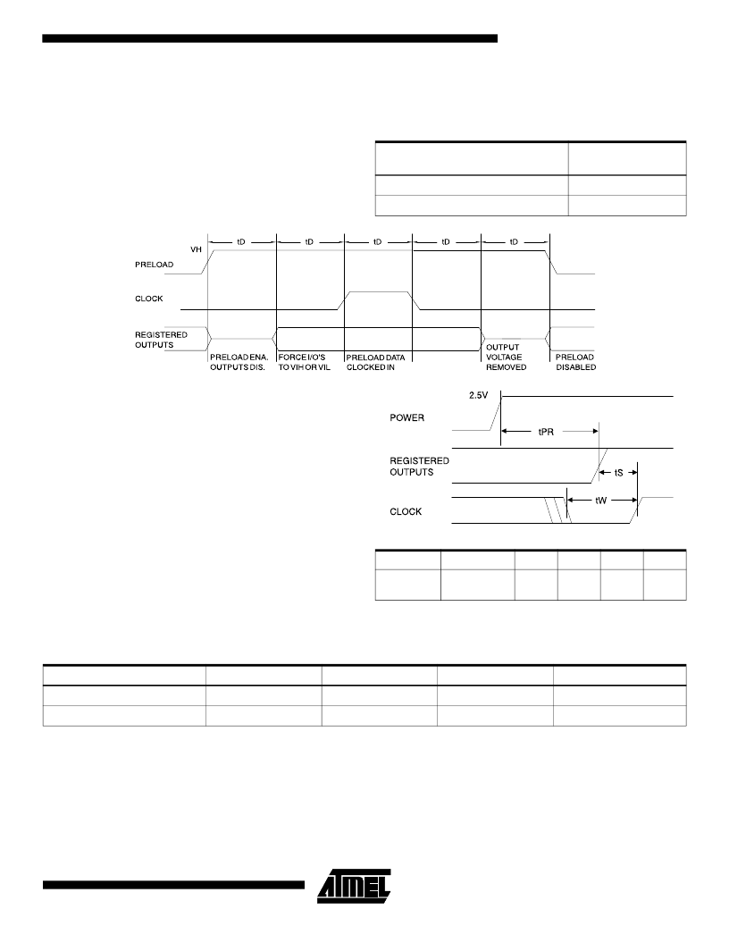
Preload of Registered Outputs
The registers in the AT22LV10 and AT22LV10L are pro-
vided with circuitry to allow loading of each register
asynchronously with either a high or a low. This feature will
simplify testing since any state can be forced into the regis-
ters to control test sequencing. A V
IH
level on the I/O pin
will force the register high; a V
IL
will force it low, indepen-
dent of the polarity bit (C0) setting. The preload state is
entered by placing an 11.5V to 13V signal on pin 8 on
DIPs, and pin 10 on SMPs. When the clock pin is pulsed
high, the data on the I/O pins is placed into the ten
registers.
Power-up Reset
The registers in the AT22LV10 and AT22LV10L are
designed to reset during power-up. At a point delayed
slightly from V
CC
crossing 2.5V, all registers will be reset to
the low state. The output state will depend on the polarity of
the output buffer.
This feature is critical for state machine initialization.
However, due to the asynchronous nature of reset and the
uncertainty of how V
CC
actually rises in the system, the
following conditions are required:
1.
The V
CC
rise must be monotonis;
2.
After reset occurs, all input and feedback setup
times must be met before driving the clock pin high,
and
3.
The clock must remain stable during t
PR
.
Note:
Erasure Characteri
s
tics
The entire fuse array of an AT22LV10 or AT22LV10L is
erased after exposure to ultraviolet light at a wavelength of
2537
. Complete erasure is assured after a minimum of
20 minutes exposure using 12,000 μW/cm
2
intensity lamps
spaced one inch away from the chip. Minimum erase time
for lamps at other intensity ratings can be calculated from
1. Typical values for nominal supply voltage. This parameter is only sampled and is not 100% tested.
the minimum integrated erasure dose of 15 W
sec/cm
2
. To
prevent unintentional erasure, an opaque label is recom-
mended to cover the clear window on any UV erasable
PLD which will be subjected to continuous fluorescent
indoor lighting or sunlight.
Level Forced on Registered Output
Pin During Preload Cycle
Register State After
Cycle
V
IH
High
V
IL
Low
Parameter
Description
Min
Typ
Max
Units
t
PR
Power-up
Reset Time
600
1000
ns
Pin Capacitance
(f = 1 MHz, T = 25
°
C)
(1)
Typ
Max
Units
Conditions
C
IN
5
8
pF
V
IN
= 0V
C
OUT
6
8
pF
V
OUT
= 0V
相关PDF资料 |
PDF描述 |
|---|---|
| AT22LV10L-35GM | UV-Erasable/OTP PLD |
| AT22LV10L-35JC | UV-Erasable/OTP PLD |
| AT22LV10L-35JI | UV-Erasable/OTP PLD |
| AT22LV10-30GC | UV-Erasable/OTP PLD |
| AT22LV10-30GI | UV-Erasable/OTP PLD |
相关代理商/技术参数 |
参数描述 |
|---|---|
| AT22LV10L-35GM | 制造商:未知厂家 制造商全称:未知厂家 功能描述:UV-Erasable/OTP PLD |
| AT22LV10L-35GM/883 | 制造商:未知厂家 制造商全称:未知厂家 功能描述:UV-Erasable/OTP PLD |
| AT22LV10L-35JC | 制造商:未知厂家 制造商全称:未知厂家 功能描述:UV-Erasable/OTP PLD |
| AT22LV10L-35JI | 制造商:未知厂家 制造商全称:未知厂家 功能描述:UV-Erasable/OTP PLD |
| AT22LV10L-35KC | 制造商:未知厂家 制造商全称:未知厂家 功能描述:UV-Erasable/OTP PLD |
发布紧急采购,3分钟左右您将得到回复。